Xerox 3300MFP Service Manual - Page 70
SMPS & HVPS board, HVPS High Voltage Power Supply
 |
UPC - 095205744415
View all Xerox 3300MFP manuals
Add to My Manuals
Save this manual to your list of manuals |
Page 70 highlights
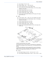
Theory of Operation SMPS & HVPS board The SMPS supplies DC Power to the System. It takes 110 V/220 V and outputs the +5 V, +24 V to supply the power to the Control Board. The HVPS board creates the high voltage of THV/MHV/Supply/Dev and supplies it to the print cartridge for making best condition to display the image. The HVPS takes the 24 V and outputs the high voltage for THV/MHV/BIAS, and the high voltage output is supplied to the toner, OPC cartridge, and transfer roller. 1) HVPS (High Voltage Power Supply) ■ Transfer High Voltage (THV+) ■ Input Voltage: 24 V DC ± 15% ■ Output Voltage: MAX +5.0 KV ± 5%, (Duty Variable, no loading) -> 1.2 KV ± 15% (when cleaning, 200 ΜΩ) ■ Output Voltage Trigger: 6.5 µΑ ■ Input contrast of the Voltage stability degree: under ± 5% (fluctuating input 21.6 V - 26.4 V) Loading contrast: ± 5% or less ■ Output Voltage Rising Time: 100 ms Max ■ Output Voltage Falling Time: 100 ms Max ■ Fluctuating transfer voltage with environmental various: +650 V (Duty 10%) ~ 5 KV (Duty 90%) ■ Environment Recognition Control Method: The THV-PWM ACTIVE is transfer active signal. It detects the resistance by recognizing the voltage value, F/B, while permits the environmental recognition voltage. ■ Output Voltage Control Method: Transfer Output Voltage is outputted and controlled by changing Duty of THVPWM Signal. 10% Duty: +650 V, 90% Duty: +5 KV ± 5% ■ Charge Voltage (MHV) ■ Input Voltage: 24 V DC ± 15% ■ Output Voltage: -1.3 KV ~ -1.8 KV DC ± 50 V ■ Output Voltage Rising Time: 50 ms Max ■ Output Voltage Falling Time: 50 ms Max ■ Output Loading range: 30 ΜΩ ~ 1000 ΜΩ ■ Output Control Signal (MHV-PWM): CPU is HV output when PWM is Low ■ Cleaning Voltage (THV-) ■ The (+) Transfer Voltage is not outputted because the THV PWM is controlled with high. ■ The (-) Transfer Voltage is outputted because the THV-Enable Signal is controlled with low. ■ The output fluctuation range is big because there is no Feedback control. ■ Developing Voltage (DEV) 2-28 Phaser 3300MFP Service Manual
-
 1
1 -
2
-
3
-
4
-
5
-
6
-
7
-
8
-
9
-
10
-
11
-
12
-
13
-
14
-
15
-
16
-
17
-
18
-
19
-
20
-
21
-
22
-
23
-
24
-
25
-
26
-
27
-
28
-
29
-
30
-
31
-
32
-
33
-
34
-
35
-
36
-
37
-
38
-
39
-
40
-
41
-
42
-
43
-
44
-
45
-
46
-
47
-
48
-
49
-
50
-
51
-
52
-
53
-
54
-
55
-
56
-
57
-
58
-
59
-
60
-
61
-
62
-
63
-
64
-
 65
65 -
 66
66 -
 67
67 -
 68
68 -
 69
69 -
 70
70 -
 71
71 -
 72
72 -
 73
73 -
 74
74 -
 75
75 -
76
-
77
-
78
-
79
-
80
-
81
-
82
-
83
-
84
-
85
-
86
-
87
-
88
-
89
-
90
-
91
-
92
-
93
-
94
-
95
-
96
-
97
-
98
-
99
-
100
-
101
-
102
-
103
-
104
-
105
-
106
-
107
-
108
-
109
-
110
-
111
-
112
-
113
-
114
-
115
-
116
-
117
-
118
-
119
-
120
-
121
-
122
-
123
-
124
-
125
-
126
-
127
-
128
-
129
-
130
-
131
-
132
-
133
-
134
-
135
-
136
-
137
-
138
-
139
-
140
-
141
-
142
-
143
-
144
-
145
-
146
-
147
-
148
-
149
-
150
-
151
-
152
-
153
-
154
-
155
-
156
-
157
-
158
-
159
-
160
-
161
-
162
-
163
-
164
-
165
-
166
-
167
-
168
-
169
-
170
-
171
-
172
-
173
-
174
-
175
-
176
-
177
-
178
-
179
-
180
-
181
-
182
-
183
-
184
-
185
-
186
-
187
-
188
-
189
-
190
-
191
-
192
-
193
-
194
-
195
-
196
-
197
-
198
-
199
-
200
-
201
-
202
-
203
-
204
-
205
-
206
-
207
-
208
-
209
-
210
-
211
-
212
-
213
-
214
-
215
-
216
-
217
-
218
-
219
-
220
-
221
-
222
-
223
-
224
-
225
-
226
-
227
-
228
-
229
-
230
-
231
-
232
-
233
-
234
-
235
-
236
-
237
-
238
-
239
-
240
-
241
-
242
-
243
-
244
-
245
-
246
-
247
-
248
-
249
-
250
-
251
-
252
-
253
-
254
-
255
-
256
-
257
-
258
-
259
-
260
-
261
-
262
-
263
-
264
-
265
-
266
-
267
-
268
-
269
-
270
-
271
-
272
-
273
-
274
-
275
-
276
-
277
-
278
-
279
-
280
-
281
-
282
-
283
-
284
-
285
-
286
-
287
-
288
-
289
-
290
-
291
-
292
-
293
-
294
-
295
-
296
 |
 |