Intel BX80605X3430 Data Sheet - Page 53

PCI Express* Based Interface Signals, DMI-Processor to PCH Serial Interface
Page 53 highlights

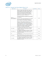
Signal Description Table 6-5. Reset and Miscellaneous Signals (Sheet 2 of 2) Signal Name RESET_OBS# Description This signal is an indication of the processor being reset. Direction O RSTIN# RSVD RSVD_NCTF RSVD_TP SM_DRAMRST# Reset In: When asserted, this signal will asynchronously reset the processor logic. This signal is connected to the I PLTRST# output of the PCH. RESERVED. Must be left unconnected on the board. Intel does not recommend a test point on the board for this land. RESERVED/Non-Critical to Function: Pin for package mechanical reliability. A test point may be placed on the board for this land. RESERVED-Test Point. A test point may be placed on the board for this land. DDR3 DRAM Reset: Reset signal from processor to DRAM devices. One common to all channels. O Type Asynch CMOS CMOS DDR3 6.4 PCI Express* Based Interface Signals Table 6-6. PCI Express* Based Interface Signals Signal Name PEG_ICOMPI PEG_ICOMPO PEG_RBIAS PEG_RCOMPO PEG_RX[15:0] PEG_RX#[15:0] PEG_TX[15:0] PEG_TX#[15:0] Description PCI Express Current Compensation. PCI Express Current Compensation. PCI Express Resistor Bias Control. PCI Express Resistance Compensation. PCI Express Receive Differential Pair. PCI Express Transmit Differential Pair. Direction I I I I I O Type Analog Analog Analog Analog PCI Express PCI Express 6.5 DMI-Processor to PCH Serial Interface Table 6-7. DMI-Processor to PCH Serial Interface Signal Name DMI_RX[3:0] DMI_RX#[3:0] DMI_TX[3:0] DMI_TX#[3:0] Description DMI input from PCH: Direct Media Interface receive differential pair. DMI output to PCH: Direct Media Interface transmit differential pair. Direction I O Type DMI DMI Datasheet, Volume 1 53

  • 1
  • 2
  • 3
  • 4
  • 5
  • 6
  • 7
  • 8
  • 9
  • 10
  • 11
  • 12
  • 13
  • 14
  • 15
  • 16
  • 17
  • 18
  • 19
  • 20
  • 21
  • 22
  • 23
  • 24
  • 25
  • 26
  • 27
  • 28
  • 29
  • 30
  • 31
  • 32
  • 33
  • 34
  • 35
  • 36
  • 37
  • 38
  • 39
  • 40
  • 41
  • 42
  • 43
  • 44
  • 45
  • 46
  • 47
  • 48
  • 49
  • 50
  • 51
  • 52
  • 53
  • 54
  • 55
  • 56
  • 57
  • 58
  • 59
  • 60
  • 61
  • 62
  • 63
  • 64
  • 65
  • 66
  • 67
  • 68
  • 69
  • 70
  • 71
  • 72
  • 73
  • 74
  • 75
  • 76
  • 77
  • 78
  • 79
  • 80
  • 81
  • 82
  • 83
  • 84
  • 85
  • 86
  • 87
  • 88
  • 89
  • 90
  • 91
  • 92
  • 93
  • 94
  • 95
  • 96
  • 97
  • 98

Datasheet, Volume 1
53
Signal Description
6.4
PCI Express* Based Interface Signals
6.5
DMI—Processor to PCH Serial Interface
RESET_OBS#
This signal is an indication of the processor being reset.
O
Asynch
CMOS
RSTIN#
Reset In: When asserted, this signal will asynchronously
reset the processor logic. This signal is connected to the
PLTRST# output of the PCH.
I
CMOS
RSVD
RESERVED. Must be left unconnected on the board.
Intel does not recommend a test point on the board for
this land.
RSVD_NCTF
RESERVED/Non-Critical to Function: Pin for package
mechanical reliability. A test point may be placed on the
board for this land.
RSVD_TP
RESERVED-Test Point. A test point may be placed on the
board for this land.
SM_DRAMRST#
DDR3 DRAM Reset: Reset signal from processor to
DRAM devices. One common to all channels.
O
DDR3
Table 6-6.
PCI Express* Based Interface Signals
Signal Name
Description
Direction
Type
PEG_ICOMPI
PCI Express Current Compensation.
I
Analog
PEG_ICOMPO
PCI Express Current Compensation.
I
Analog
PEG_RBIAS
PCI Express Resistor Bias Control.
I
Analog
PEG_RCOMPO
PCI Express Resistance Compensation.
I
Analog
PEG_RX[15:0]
PEG_RX#[15:0]
PCI Express Receive Differential Pair.
I
PCI
Express
PEG_TX[15:0]
PEG_TX#[15:0]
PCI Express Transmit Differential Pair.
O
PCI
Express
Table 6-7.
DMI—Processor to PCH Serial Interface
Signal Name
Description
Direction
Type
DMI_RX[3:0]
DMI_RX#[3:0]
DMI input from PCH: Direct Media Interface receive
differential pair.
I
DMI
DMI_TX[3:0]
DMI_TX#[3:0]
DMI output to PCH: Direct Media Interface transmit
differential pair.
O
DMI
Table 6-5.
Reset and Miscellaneous Signals (Sheet 2 of 2)
Signal Name
Description
Direction
Type