Intel BX80605X3430 Data Sheet - Page 72
Notes
 |
UPC - 735858210331
View all Intel BX80605X3430 manuals
Add to My Manuals
Save this manual to your list of manuals |
Page 72 highlights
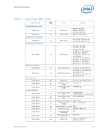
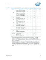
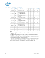
Electrical Specifications Table 7-7. VCC Static and Transient Tolerance Voltage Deviation from VID Setting 1, 2, 3 ICC (A) VCC_Max (V) 1.40 m VCC_Typ (V) 1.40 m VCC_Min (V) 1.40 m 0 0.000 -0.019 -0.038 5 -0.007 -0.026 -0.045 10 -0.014 -0.033 -0.052 15 -0.021 -0.040 -0.059 20 -0.028 -0.047 -0.066 25 -0.035 -0.054 -0.073 30 -0.042 -0.061 -0.080 35 -0.049 -0.068 -0.087 40 -0.056 -0.075 -0.094 45 -0.063 -0.082 -0.101 50 -0.070 -0.089 -0.108 55 -0.077 -0.096 -0.115 60 -0.084 -0.103 -0.122 65 -0.091 -0.110 -0.129 70 -0.098 -0.117 -0.136 75 -0.105 -0.124 -0.143 80 -0.112 -0.131 -0.150 85 -0.119 -0.138 -0.157 90 -0.126 -0.145 -0.164 95 -0.133 -0.152 -0.171 100 -0.140 -0.159 -0.178 110 -0.147 -0.166 -0.185 Notes: 1. The VCC_MIN and VCC_MAX loadlines represent static and transient limits. 2. This table is intended to aid in reading discrete points on Figure 7-1. 3. The loadlines specify voltage limits at the die measured at the VCC_SENSE and VSS_SENSE lands. Voltage regulation feedback for voltage regulator circuits must also be taken from processor VCC_SENSE and VSS_SENSE lands. Refer to the Voltage Regulator Down (VRD) 11.1 Design Guidelines for socket load line guidelines and VR implementation. 72 Datasheet, Volume 1
-
 1
1 -
2
-
3
-
4
-
5
-
6
-
7
-
8
-
9
-
10
-
11
-
12
-
13
-
14
-
15
-
16
-
17
-
18
-
19
-
20
-
21
-
22
-
23
-
24
-
25
-
26
-
27
-
28
-
29
-
30
-
31
-
32
-
33
-
34
-
35
-
36
-
37
-
38
-
39
-
40
-
41
-
42
-
43
-
44
-
45
-
46
-
47
-
48
-
49
-
50
-
51
-
52
-
53
-
54
-
55
-
56
-
57
-
58
-
59
-
60
-
61
-
62
-
63
-
64
-
65
-
66
-
 67
67 -
 68
68 -
 69
69 -
 70
70 -
 71
71 -
 72
72 -
 73
73 -
 74
74 -
 75
75 -
 76
76 -
 77
77 -
78
-
79
-
80
-
81
-
82
-
83
-
84
-
85
-
86
-
87
-
88
-
89
-
90
-
91
-
92
-
93
-
94
-
95
-
96
-
97
-
98
 |
 |
