Intel BX80605X3430 Data Sheet - Page 74
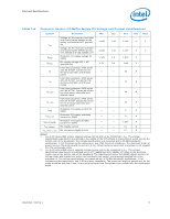
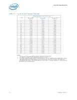
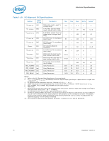
Table 7-8., DDR3 Signal Group DC Specifications
 |
UPC - 735858210331
View all Intel BX80605X3430 manuals
Add to My Manuals
Save this manual to your list of manuals |
Page 74 highlights
Electrical Specifications Table 7-8. DDR3 Signal Group DC Specifications Symbol VIL VIH VOL VOH RON RON RON RON Data ODT ILI SM_RCOMP0 SM_RCOMP1 SM_RCOMP2 Parameter Input Low Voltage Input High Voltage Output Low Voltage Output High Voltage DDR3 Clock Buffer On Resistance DDR3 Command Buffer On Resistance DDR3 Control Buffer On Resistance DDR3 Data Buffer On Resistance On-Die Termination for Data Signals Input Leakage Current COMP Resistance COMP Resistance COMP Resistance Alpha Group (e,f) (e,f) (c,d,e,f) (c,d,e,f) - - - - (d) - (t) (t) (t) Min Typ Max Units Notes1 - - 0.43*VDDQ V 2,4 0.57*VDDQ - - V 3 - ((VRDODNQ+R/ V2T)T*_T(ERROMN))/ - 6 - (RVODND/Q(R-ON((+VRDVDTQT_/TE2R)M*)) - V 4,6 21 - 36 5 20 - 31 5 20 - 31 5 21 - 36 5 93.5 - 99 24.7 128.7 - - 100 24.9 130 126.5 ± 1 mA 101 7 25.1 7 131.3 7 Notes: 1. Unless otherwise noted, all specifications in this table apply to all processor frequencies. 2. VIL is defined as the maximum voltage level at a receiving agent that will be interpreted as a logical low value. 3. VIH is defined as the minimum voltage level at a receiving agent that will be interpreted as a logical high value. 4. VIH and VOH may experience excursions above VDDQ. However, input signal drivers must comply with the signal quality specifications. 5. This is the pull down driver resistance. 6. RVTT_TERM is the termination on the DIMM and is not controlled by the processor. 7. COMP resistance must be provided on the system board with 1% resistors. COMP resistors are to VSS. 74 Datasheet, Volume 1
-
 1
1 -
2
-
3
-
4
-
5
-
6
-
7
-
8
-
9
-
10
-
11
-
12
-
13
-
14
-
15
-
16
-
17
-
18
-
19
-
20
-
21
-
22
-
23
-
24
-
25
-
26
-
27
-
28
-
29
-
30
-
31
-
32
-
33
-
34
-
35
-
36
-
37
-
38
-
39
-
40
-
41
-
42
-
43
-
44
-
45
-
46
-
47
-
48
-
49
-
50
-
51
-
52
-
53
-
54
-
55
-
56
-
57
-
58
-
59
-
60
-
61
-
62
-
63
-
64
-
65
-
66
-
67
-
68
-
 69
69 -
 70
70 -
 71
71 -
 72
72 -
 73
73 -
 74
74 -
 75
75 -
 76
76 -
 77
77 -
 78
78 -
 79
79 -
80
-
81
-
82
-
83
-
84
-
85
-
86
-
87
-
88
-
89
-
90
-
91
-
92
-
93
-
94
-
95
-
96
-
97
-
98
 |
 |
