Intel BX80605X3430 Data Sheet - Page 62
PLL Power Supply
 |
UPC - 735858210331
View all Intel BX80605X3430 manuals
Add to My Manuals
Save this manual to your list of manuals |
Page 62 highlights
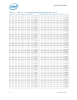
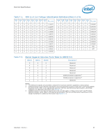
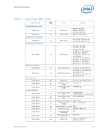
Electrical Specifications 7.3 7.3.1 7.4 Note: Processor Clocking (BCLK[0], BCLK#[0]) The processor uses a differential clock to generate the processor core(s) operating frequency, memory controller frequency, and other internal clocks. The processor core frequency is determined by multiplying the processor core ratio by 133 MHz. Clock multiplying within the processor is provided by an internal phase locked loop (PLL) that requires a constant frequency input, with exceptions for Spread Spectrum Clocking (SSC). The processor maximum core frequency is configured during power-on reset by using its manufacturing default value. This value is the highest core multiplier at which the processor can operate. If lower maximum speeds are desired, the appropriate ratio can be configured using the FLEX_RATIO MSR. PLL Power Supply An on-die PLL filter solution is implemented on the processor. Refer to Table 7-6 for DC specifications. VCC Voltage Identification (VID) The VID specification for the processor is defined by the Voltage Regulator Down (VRD) 11.1 Design Guidelines. The processor uses eight voltage identification signals, VID[7:0], to support automatic selection of voltages. Table 7-1 specifies the voltage level corresponding to the state of VID[7:0]. A '1' in this table refers to a high voltage level and a '0' refers to a low voltage level. If the processor socket is empty (VID[7:0] = 11111111), or the voltage regulation circuit cannot supply the voltage that is requested, the voltage regulator must disable itself. See the Voltage Regulator Down (VRD) 11.1 Design Guidelines for further details. VID signals are CMOS push/pull drivers. Refer to Table 7-9 for the DC specifications for these signals. The VID codes will change due to temperature and/or current load changes to minimize the power of the part. A voltage range is provided in Table 7-5. The specifications are set so that one voltage regulator can operate with all supported frequencies. Individual processor VID values may be set during manufacturing so that two devices at the same core frequency may have different default VID settings. This is shown in the VID range values in Table 7-5. The processor provides the ability to operate while transitioning to an adjacent VID and its associated processor core voltage (VCC). This will represent a DC shift in the loadline. A low-to-high or high-to-low voltage state change will result in as many VID transitions as necessary to reach the target core voltage. Transitions above the maximum specified VID are not permitted. One VID transition occurs in 1.25 us. Table 7-1 includes VID step sizes and DC shift ranges. Minimum and maximum voltages must be maintained. The VR used must be capable of regulating its output to the value defined by the new VID values issued. DC specifications for dynamic VID transitions are included in Table 7-5 and Table 7-7. See the Voltage Regulator Down (VRD) 11.1 Design Guidelines for further details. Several of the VID signals (VID[5:3]/CSC[2:0] and VID[2:0]/MSID[2:0]) serve a dual purpose and are sampled during reset. Refer to the signal description table in Chapter 6 and Table 7-3 for further information. 62 Datasheet, Volume 1
-
 1
1 -
2
-
3
-
4
-
5
-
6
-
7
-
8
-
9
-
10
-
11
-
12
-
13
-
14
-
15
-
16
-
17
-
18
-
19
-
20
-
21
-
22
-
23
-
24
-
25
-
26
-
27
-
28
-
29
-
30
-
31
-
32
-
33
-
34
-
35
-
36
-
37
-
38
-
39
-
40
-
41
-
42
-
43
-
44
-
45
-
46
-
47
-
48
-
49
-
50
-
51
-
52
-
53
-
54
-
55
-
56
-
 57
57 -
 58
58 -
 59
59 -
 60
60 -
 61
61 -
 62
62 -
 63
63 -
 64
64 -
 65
65 -
 66
66 -
 67
67 -
68
-
69
-
70
-
71
-
72
-
73
-
74
-
75
-
76
-
77
-
78
-
79
-
80
-
81
-
82
-
83
-
84
-
85
-
86
-
87
-
88
-
89
-
90
-
91
-
92
-
93
-
94
-
95
-
96
-
97
-
98
 |
 |