Intel P8700 Data Sheet - Page 76
Power/Other
 |
UPC - 735858206174
View all Intel P8700 manuals
Add to My Manuals
Save this manual to your list of manuals |
Page 76 highlights
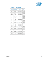
Package Mechanical Specifications and Pin Information Table 17. Pin # Listing Pin # Pin Name Signal Buffer Type Directi on F2 F3 F4 F5 F6 F7 F8 F9 F10 F11 F12 F13 F14 F15 F16 F17 F18 F19 F20 F21 F22 F23 F24 F25 F26 G1 G2 G3 G4 G5 G6 G21 G22 G23 G24 VSS RS[0]# RS[1]# VSS RSVD VCC VSS VCC VCC VSS VCC VSS VCC VCC VSS VCC VCC VSS VCC DRDY# VSS D[4]# D[1]# VSS D[13]# VSS TRDY# RS[2]# VSS BPRI# HIT# VCCP D[3]# VSS D[9]# Power/Other Common Clock Input Common Clock Input Power/Other Reserved Power/Other Power/Other Power/Other Power/Other Power/Other Power/Other Power/Other Power/Other Power/Other Power/Other Power/Other Power/Other Power/Other Power/Other Common Clock Input/ Output Power/Other Source Synch Input/ Output Source Synch Input/ Output Power/Other Source Synch Input/ Output Power/Other Common Clock Input Common Clock Input Power/Other Common Clock Input Common Clock Input/ Output Power/Other Source Synch Input/ Output Power/Other Source Synch Input/ Output Table 17. Pin # Listing Pin # Pin Name Signal Buffer Type Directi on G25 G26 H1 H2 H3 H4 H5 H6 H21 H22 H23 H24 H25 H26 J1 J2 J3 J4 J5 J6 J21 J22 J23 J24 J25 J26 K1 K2 D[5]# Source Synch Input/ Output VSS Power/Other ADS# Common Clock Input/ Output REQ[1]# Source Synch Input/ Output VSS Power/Other LOCK# Common Clock Input/ Output DEFER# Common Clock Input VSS Power/Other VSS Power/Other D[12]# Source Synch Input/ Output D[15]# Source Synch Input/ Output VSS Power/Other DINV[0]# Source Synch Input/ Output DSTBP[0] # Source Synch Input/ Output A[9]# Source Synch Input/ Output VSS Power/Other REQ[3]# Source Synch Input/ Output A[3]# Source Synch Input/ Output VSS Power/Other VCCP Power/Other VCCP Power/Other VSS Power/Other D[11]# Source Synch Input/ Output D[10]# Source Synch Input/ Output VSS Power/Other DSTBN[0] # Source Synch Input/ Output VSS Power/Other REQ[2]# Source Synch Input/ Output 76 Datasheet
-
 1
1 -
2
-
3
-
4
-
5
-
6
-
7
-
8
-
9
-
10
-
11
-
12
-
13
-
14
-
15
-
16
-
17
-
18
-
19
-
20
-
21
-
22
-
23
-
24
-
25
-
26
-
27
-
28
-
29
-
30
-
31
-
32
-
33
-
34
-
35
-
36
-
37
-
38
-
39
-
40
-
41
-
42
-
43
-
44
-
45
-
46
-
47
-
48
-
49
-
50
-
51
-
52
-
53
-
54
-
55
-
56
-
57
-
58
-
59
-
60
-
61
-
62
-
63
-
64
-
65
-
66
-
67
-
68
-
69
-
70
-
 71
71 -
 72
72 -
 73
73 -
 74
74 -
 75
75 -
 76
76 -
 77
77 -
 78
78 -
 79
79 -
 80
80 -
 81
81 -
82
-
83
-
84
-
85
-
86
-
87
-
88
-
89
-
90
-
91
-
92
-
93
-
94
-
95
-
96
-
97
-
98
-
99
-
100
-
101
-
102
-
103
-
104
-
105
-
106
-
107
-
108
-
109
-
110
-
111
-
112
-
113
 |
 |
