Intel 521 Data Sheet - Page 21
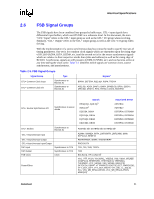
FSB Signal Groups
 |
UPC - 683728199029
View all Intel 521 manuals
Add to My Manuals
Save this manual to your list of manuals |
Page 21 highlights
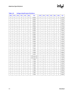
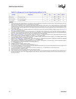
Electrical Specifications 2.6 FSB Signal Groups The FSB signals have been combined into groups by buffer type. GTL+ input signals have differential input buffers, which use GTLREF as a reference level. In this document, the term "GTL+ Input" refers to the GTL+ input group as well as the GTL+ I/O group when receiving. Similarly, "GTL+ Output" refers to the GTL+ output group as well as the GTL+ I/O group when driving. With the implementation of a source synchronous data bus comes the need to specify two sets of timing parameters. One set is for common clock signals which are dependent upon the rising edge of BCLK0 (ADS#, HIT#, HITM#, etc.) and the second set is for the source synchronous signals which are relative to their respective strobe lines (data and address) as well as the rising edge of BCLK0. Asychronous signals are still present (A20M#, IGNNE#, etc.) and can become active at any time during the clock cycle. Table 2-3 identifies which signals are common clock, source synchronous, and asynchronous. Table 2-3. FSB Signal Groups Signal Group GTL+ Common Clock Input GTL+ Common Clock I/O Type Synchronous to BCLK[1:0] Synchronous to BCLK[1:0] Signals1 BPRI#, DEFER#, RS[2:0]#, RSP#, TRDY# AP[1:0]#, ADS#, BINIT#, BNR#, BPM[5:0]#, BR0#, DBSY#, DP[3:0]#, DRDY#, HIT#, HITM#, LOCK#, MCERR# GTL+ Source Synchronous I/O Synchronous to assoc. strobe Signals REQ[4:0]#, A[16:3]#3 A[35:17]#3 D[15:0]#, DBI0# D[31:16]#, DBI1# D[47:32]#, DBI2# D[63:48]#, DBI3# Associated Strobe ADSTB0# ADSTB1# DSTBP0#, DSTBN0# DSTBP1#, DSTBN1# DSTBP2#, DSTBN2# DSTBP3#, DSTBN3# GTL+ Strobes Synchronous to BCLK[1:0] GTL+ Asynchronous Input GTL+ Asynchronous Output GTL+ Asynchronous Input/Output TAP Input TAP Output FSB Clock Synchronous to TCK Synchronous to TCK Clock Power/Other ADSTB[1:0]#, DSTBP[3:0]#, DSTBN[3:0]# A20M#, IGNNE#, INIT#, LINT0/INTR, LINT1/NMI, SMI#, STPCLK#, RESET# FERR#/PBE#, IERR#, THERMTRIP# PROCHOT# TCK, TDI, TMS, TRST# TDO BCLK[1:0], ITP_CLK[1:0]2 VCC, VTT, VCCA, VCCIOPLL, VID[5:0], VSS, VSSA, GTLREF, COMP[1:0], RESERVED, TESTHI[13:0], THERMDA, THERMDC, VCC_SENSE, VSS_SENSE, BSEL[2:0], SKTOCC#, DBR#2, VTTPWRGD, BOOTSELECT, PWRGOOD, VTT_OUT_LEFT, VTT_OUT_RIGHT, VTT_SEL, LL_ID[1:0], FCx, VSS_MB_REGULATION, VCC_MB_REGULATION, MSID[1:0] Datasheet 21
-
 1
1 -
2
-
3
-
4
-
5
-
6
-
7
-
8
-
9
-
10
-
11
-
12
-
13
-
14
-
15
-
 16
16 -
 17
17 -
 18
18 -
 19
19 -
 20
20 -
 21
21 -
 22
22 -
 23
23 -
 24
24 -
 25
25 -
 26
26 -
27
-
28
-
29
-
30
-
31
-
32
-
33
-
34
-
35
-
36
-
37
-
38
-
39
-
40
-
41
-
42
-
43
-
44
-
45
-
46
-
47
-
48
-
49
-
50
-
51
-
52
-
53
-
54
-
55
-
56
-
57
-
58
-
59
-
60
-
61
-
62
-
63
-
64
-
65
-
66
-
67
-
68
-
69
-
70
-
71
-
72
-
73
-
74
-
75
-
76
-
77
-
78
-
79
-
80
-
81
-
82
-
83
-
84
-
85
-
86
-
87
-
88
-
89
-
90
-
91
-
92
-
93
-
94
-
95
-
96
 |
 |
