Intel 521 Data Sheet - Page 32
Table 2-13. PWRGOOD and TAP Signal Group DC Specifications - vt
 |
UPC - 683728199029
View all Intel 521 manuals
Add to My Manuals
Save this manual to your list of manuals |
Page 32 highlights
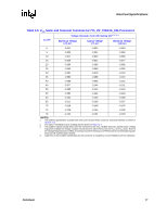
Electrical Specifications Table 2-13. PWRGOOD and TAP Signal Group DC Specifications Symbol Parameter Min Max Unit Notes1, 2 VHYS VT+ Input Hysteresis Input low to high threshold voltage 200 350 mV 3 0.5 * (VTT + VHYS_MIN) 0.5 * (VTT + VHYS_MAX) V 4 VT- Input high to low threshold voltage 0.5 * (VTT - VHYS_MAX) 0.5 * (VTT - VHYS_MIN) V 4 VOH Output High Voltage N/A IOL Output Low Current - ILI Input Leakage Current - ILO Output Leakage Current - VTT 45 ± 200 ± 200 V 4 mA 5 µA 6 µA - RON Buffer On Resistance 7 12 Ω - NOTES: 1. Unless otherwise noted, all specifications in this table apply to all processor frequencies. 2. All outputs are open drain. 3. VHYS represents the amount of hysteresis, nominally centered about 0.5 * VTT, for all TAP inputs. 4. The VTT referred to in these specifications refers to instantaneous VTT. 5. The maximum output current is based on maximum current handling capability of the buffer and is not specified into the test load. 6. Leakage to VSS with land held at VTT. Table 2-14. VTTPWRGD DC Specifications Symbol VIL VIH Parameter Input Low Voltage Input High Voltage Min Typ Max Unit - - 0.3 V 0.9 - - V Notes Table 2-15. BSEL [2:0] and VID[5:0] DC Specifications Symbol Parameter Max Unit Notes1, 2 RON (BSEL) Buffer On Resistance 60 Ω - RON (VID) Buffer On Resistance 60 Ω - IOL Max Land Current ILO Output Leakage Current 8 mA - 200 µA 3 VTOL Voltage Tolerance VTT (max) V - NOTES: 1. Unless otherwise noted, all specifications in this table apply to all processor frequencies. 2. These parameters are not tested and are based on design simulations. 3. Leakage to VSS with land held at 2.5 V. Table 2-16. BOOTSELECT DC Specifications Symbol Parameter Min Typ Max VIL Input Low Voltage - - VIH Input High Voltage 0.96 - NOTES: 1. These parameters are not tested and are based on design simulations. 0.24 - Unit V V Notes 1 - 32 Datasheet
-
 1
1 -
2
-
3
-
4
-
5
-
6
-
7
-
8
-
9
-
10
-
11
-
12
-
13
-
14
-
15
-
16
-
17
-
18
-
19
-
20
-
21
-
22
-
23
-
24
-
25
-
26
-
 27
27 -
 28
28 -
 29
29 -
 30
30 -
 31
31 -
 32
32 -
 33
33 -
 34
34 -
 35
35 -
 36
36 -
 37
37 -
38
-
39
-
40
-
41
-
42
-
43
-
44
-
45
-
46
-
47
-
48
-
49
-
50
-
51
-
52
-
53
-
54
-
55
-
56
-
57
-
58
-
59
-
60
-
61
-
62
-
63
-
64
-
65
-
66
-
67
-
68
-
69
-
70
-
71
-
72
-
73
-
74
-
75
-
76
-
77
-
78
-
79
-
80
-
81
-
82
-
83
-
84
-
85
-
86
-
87
-
88
-
89
-
90
-
91
-
92
-
93
-
94
-
95
-
96
 |
 |
