Intel 521 Data Sheet - Page 31
Table 2-11., GTL+ Asynchronous Signal Group DC Specifications, Table 2-12. GTL+ Signal Group DC
 |
UPC - 683728199029
View all Intel 521 manuals
Add to My Manuals
Save this manual to your list of manuals |
Page 31 highlights
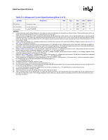
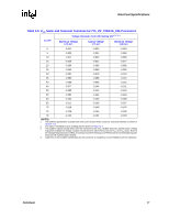
Electrical Specifications Table 2-11. GTL+ Asynchronous Signal Group DC Specifications Symbol Parameter Min Max Unit Notes1 VIL Input Low Voltage VIH Input High Voltage VOH Output High Voltage 0.0 VTT/2 + (0.10 * VTT) 0.90*VTT VTT/2 - (0.10 * VTT) VTT VTT V 2, 3 V 3, 4, 5, 6 V 5, 6, 7 IOL Output Low Current - ILI Input Leakage Current N/A ILO Output Leakage Current N/A VTT/[(0.50*RTT_MIN) + RON_MIN] ± 200 ± 200 A 8 µA 9 µA 10 RON Buffer On Resistance 8 12 Ω - NOTES: 1. Unless otherwise noted, all specifications in this table apply to all processor frequencies. 2. VIL is defined as the voltage range at a receiving agent that will be interpreted as a logical low value. 3. LINT0/INTR and LINT1/NMI use GTLREF as a reference voltage. For these two signals VIH = GTLREF + (0.10 * VTT) and VIL= GTLREF - (0.10 * VTT). 4. VIH is defined as the voltage range at a receiving agent that will be interpreted as a logical high value. 5. VIH and VOH may experience excursions above VTT. However, input signal drivers must comply with the signal quality spec- ifications. 6. The VTT referred to in these specifications refers to instantaneous VTT. 7. All outputs are open drain. 8. The maximum output current is based on maximum current handling capability of the buffer and is not specified into the test load. 9. Leakage to VSS with land held at VTT. 10. Leakage to VTT with land held at 300 mV. Table 2-12. GTL+ Signal Group DC Specifications Symbol Parameter Min Max Unit VIL Input Low Voltage 0.0 GTLREF - (0.10 * VTT) V VIH Input High Voltage GTLREF + (0.10 * VTT) VTT V VOH Output High Voltage 0.90*VTT VTT V IOL Output Low Current N/A VTT/[(0.50*RTT_MIN) + RON_MIN] A ILI Input Leakage Current N/A ± 200 µA ILO Output Leakage Current N/A ± 200 µA RON Buffer On Resistance 8 12 Ω NOTES: 1. Unless otherwise noted, all specifications in this table apply to all processor frequencies. 2. VIL is defined as the voltage range at a receiving agent that will be interpreted as a logical low value. 3. The VTT referred to in these specifications is the instantaneous VTT. 4. VIH is defined as the voltage range at a receiving agent that will be interpreted as a logical high value. 5. Leakage to VSS with land held at VTT. Notes1 2, 3 3, 4 3 - 5 - - Datasheet 31
-
 1
1 -
2
-
3
-
4
-
5
-
6
-
7
-
8
-
9
-
10
-
11
-
12
-
13
-
14
-
15
-
16
-
17
-
18
-
19
-
20
-
21
-
22
-
23
-
24
-
25
-
 26
26 -
 27
27 -
 28
28 -
 29
29 -
 30
30 -
 31
31 -
 32
32 -
 33
33 -
 34
34 -
 35
35 -
 36
36 -
37
-
38
-
39
-
40
-
41
-
42
-
43
-
44
-
45
-
46
-
47
-
48
-
49
-
50
-
51
-
52
-
53
-
54
-
55
-
56
-
57
-
58
-
59
-
60
-
61
-
62
-
63
-
64
-
65
-
66
-
67
-
68
-
69
-
70
-
71
-
72
-
73
-
74
-
75
-
76
-
77
-
78
-
79
-
80
-
81
-
82
-
83
-
84
-
85
-
86
-
87
-
88
-
89
-
90
-
91
-
92
-
93
-
94
-
95
-
96
 |
 |
