Intel 521 Data Sheet - Page 73
Table 4-3. Signal Description, Sheet 8 of 8
 |
UPC - 683728199029
View all Intel 521 manuals
Add to My Manuals
Save this manual to your list of manuals |
Page 73 highlights
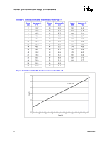
Land Listing and Signal Descriptions Table 4-3. Signal Description (Sheet 8 of 8) Name Type Description VID[5:0] Output VID[5:0] (Voltage ID) signals are used to support automatic selection of power supply voltages (VCC). These are open drain signals that are driven by the processor and must be pulled up on the motherboard. Refer to the Voltage Regulator-Down (VRD) 10.1 Design Guide for Desktop Socket 775 for more information. The voltage supply for these signals must be valid before the VR can supply VCC to the processor. Conversely, the VR output must be disabled until the voltage supply for the VID signals becomes valid. The VID signals are needed to support the processor voltage specification variations. See Table 2-2 for definitions of these signals. The VR must supply the voltage that is requested by the signals, or disable itself. VSS Input VSS are the ground pins for the processor and should be connected to the system ground plane. VSSA Input VSSA is the isolated ground for internal PLLs. VSS_SENSE Output VSS_SENSE is an isolated low impedance connection to processor core VSS. It can be used to sense or measure ground near the silicon with little noise. VSS_MB_ REGULATION Output This land is provided as a voltage regulator feedback sense point for VSS. It is connected internally in the processor package to the sense point land V27 as described in the Voltage Regulator-Down (VRD) 10.1 Design Guide for Desktop Socket 775. VTT Miscellaneous voltage supply. VTT_OUT_LEFT VTT_OUT_RIGHT Output The VTT_OUT_LEFT and VTT_OUT_RIGHT signals are included to provide a voltage supply for some signals that require termination to VTT on the motherboard. For future processor compatibility some signals are required to be pulled up to VTT_OUT_LEFT or VTT_OUT_RIGHT. Refer to the following table for the signals that should be pulled up to VTT_OUT_LEFT and VTT_OUT_RIGHT. Pull-up Signal Signals to be Pulled Up VTT_OUT_RIGHT VTT_PWRGOOD, VID[5:0], GTLREF, TMS, TDI, TDO, BPM[5:0], other VRD components VTT_OUT_LEFT RESET#, BR0#, PWRGOOD, TESTHI1, TESTHI8, TESTHI9, TESTHI10, TESTHI11, TESTHI12 VTT_SEL VTTPWRGD Output The VTT_SEL signal is used to select the correct VTT voltage level for the processor. Input The processor requires this input to determine that the VTT voltages are stable and within specification. § Datasheet 73
-
 1
1 -
2
-
3
-
4
-
5
-
6
-
7
-
8
-
9
-
10
-
11
-
12
-
13
-
14
-
15
-
16
-
17
-
18
-
19
-
20
-
21
-
22
-
23
-
24
-
25
-
26
-
27
-
28
-
29
-
30
-
31
-
32
-
33
-
34
-
35
-
36
-
37
-
38
-
39
-
40
-
41
-
42
-
43
-
44
-
45
-
46
-
47
-
48
-
49
-
50
-
51
-
52
-
53
-
54
-
55
-
56
-
57
-
58
-
59
-
60
-
61
-
62
-
63
-
64
-
65
-
66
-
67
-
 68
68 -
 69
69 -
 70
70 -
 71
71 -
 72
72 -
 73
73 -
 74
74 -
 75
75 -
 76
76 -
 77
77 -
 78
78 -
79
-
80
-
81
-
82
-
83
-
84
-
85
-
86
-
87
-
88
-
89
-
90
-
91
-
92
-
93
-
94
-
95
-
96
 |
 |
