Intel E3300 Data Sheet - Page 16
Reserved, Unused, and TESTHI Signals, Power Segment Identifier PSID
 |
View all Intel E3300 manuals
Add to My Manuals
Save this manual to your list of manuals |
Page 16 highlights
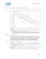
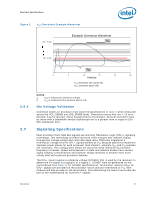
Electrical Specifications 2.4 2.5 Reserved, Unused, and TESTHI Signals All RESERVED lands must remain unconnected. Connection of these lands to VCC, VSS, VTT, or to any other signal (including each other) can result in component malfunction or incompatibility with future processors. See Chapter 4 for a land listing of the processor and the location of all RESERVED lands. In a system level design, on-die termination has been included by the processor to allow signals to be terminated within the processor silicon. Most unused GTL+ inputs should be left as no connects as GTL+ termination is provided on the processor silicon. However, see Table 7 for details on GTL+ signals that do not include on-die termination. Unused active high inputs, should be connected through a resistor to ground (VSS). Unused outputs can be left unconnected, however this may interfere with some TAP functions, complicate debug probing, and prevent boundary scan testing. A resistor must be used when tying bidirectional signals to power or ground. When tying any signal to power or ground, a resistor will also allow for system testability. Resistor values should be within ± 20% of the impedance of the motherboard trace for front side bus signals. For unused GTL+ input or I/O signals, use pull-up resistors of the same value as the on-die termination resistors (RTT). For details see Table 14. TAP and CMOS signals do not include on-die termination. Inputs and used outputs must be terminated on the motherboard. Unused outputs may be terminated on the motherboard or left unconnected. Note that leaving unused outputs unterminated may interfere with some TAP functions, complicate debug probing, and prevent boundary scan testing. All TESTHI[12,10:0] lands should be individually connected to VTT using a pull-up resistor that matches the nominal trace impedance. The TESTHI signals may use individual pull-up resistors or be grouped together as detailed below. A matched resistor must be used for each group: • TESTHI[1:0] • TESTHI[7:2] • TESTHI8/FC42 - cannot be grouped with other TESTHI signals • TESTHI9/FC43 - cannot be grouped with other TESTHI signals • TESTHI10 - cannot be grouped with other TESTHI signals • TESTHI12/FC44 - cannot be grouped with other TESTHI signals Terminating multiple TESTHI pins together with a single pull-up resistor is not recommended for designs supporting boundary scan for proper Boundary Scan testing of the TESTHI signals. For optimum noise margin, all pull-up resistor values used for TESTHI[12,10:0] lands should have a resistance value within ± 20% of the impedance of the board transmission line traces. For example, if the nominal trace impedance is 50 , then a value between 40 and 60 should be used. Power Segment Identifier (PSID) Power Segment Identifier (PSID) is a mechanism to prevent booting under mismatched power requirement situations. The PSID mechanism enables BIOS to detect if the processor in use requires more power than the platform voltage regulator (VR) is capable of supplying. For example, a 130 W TDP processor installed in a board with a 65 W or 95 W TDP capable VR may draw too much power and cause a potential VR issue. 16 Datasheet
-
 1
1 -
2
-
3
-
4
-
5
-
6
-
7
-
8
-
9
-
10
-
 11
11 -
 12
12 -
 13
13 -
 14
14 -
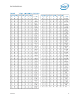 15
15 -
 16
16 -
 17
17 -
 18
18 -
 19
19 -
 20
20 -
 21
21 -
22
-
23
-
24
-
25
-
26
-
27
-
28
-
29
-
30
-
31
-
32
-
33
-
34
-
35
-
36
-
37
-
38
-
39
-
40
-
41
-
42
-
43
-
44
-
45
-
46
-
47
-
48
-
49
-
50
-
51
-
52
-
53
-
54
-
55
-
56
-
57
-
58
-
59
-
60
-
61
-
62
-
63
-
64
-
65
-
66
-
67
-
68
-
69
-
70
-
71
-
72
-
73
-
74
-
75
-
76
-
77
-
78
-
79
-
80
-
81
-
82
-
83
-
84
-
85
-
86
-
87
-
88
-
89
-
90
-
91
-
92
-
93
-
94
-
95
-
96
-
97
-
98
-
99
-
100
 |
 |
