Intel E3300 Data Sheet - Page 24
Processor DC Specifications
 |
View all Intel E3300 manuals
Add to My Manuals
Save this manual to your list of manuals |
Page 24 highlights
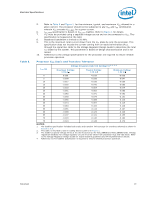
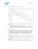
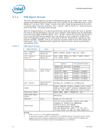
Electrical Specifications 2.7.3 Table 10. Table 11. Processor DC Specifications The processor DC specifications in this section are defined at the processor core (pads) unless otherwise stated. All specifications apply to all frequencies and cache sizes unless otherwise stated. GTL+ Signal Group DC Specifications Symbol Parameter Min Max Unit Notes1 VIL Input Low Voltage -0.10 GTLREF - 0.10 V 2, 5 VIH Input High Voltage GTLREF + 0.10 VTT + 0.10 V 3, 4, 5 VOH Output High Voltage VTT - 0.10 VTT V 4, 5 IOL Output Low Current N/A VTT_MAX / [(RTT_MIN) + (2 * RON_MIN)] A - ILI Input Leakage Current N/A ± 100 µA 6 ILO Output Leakage Current N/A ± 100 µA 7 RON Buffer On Resistance 7.49 9.16 NOTES: 1. Unless otherwise noted, all specifications in this table apply to all processor frequencies. 2. VIL is defined as the voltage range at a receiving agent that will be interpreted as a logical low value. 3. VIH is defined as the voltage range at a receiving agent that will be interpreted as a logical high value. 4. VIH and VOH may experience excursions above VTT. 5. The VTT referred to in these specifications is the instantaneous VTT. 6. Leakage to VSS with land held at VTT. 7. Leakage to VTT with land held at 300 mV. Open Drain and TAP Output Signal Group DC Specifications Symbol Parameter Min Max Unit Notes1 VOL Output Low Voltage IOL Output Low Current ILO Output Leakage Current 0 0.20 V - 16 50 mA 2 N/A ± 200 µA 3 NOTES: 1. Unless otherwise noted, all specifications in this table apply to all processor frequencies. 2. Measured at VTT * 0.2 V. 3. For Vin between 0 and VOH. 24 Datasheet
-
 1
1 -
2
-
3
-
4
-
5
-
6
-
7
-
8
-
9
-
10
-
11
-
12
-
13
-
14
-
15
-
16
-
17
-
18
-
 19
19 -
 20
20 -
 21
21 -
 22
22 -
 23
23 -
 24
24 -
 25
25 -
 26
26 -
 27
27 -
 28
28 -
 29
29 -
30
-
31
-
32
-
33
-
34
-
35
-
36
-
37
-
38
-
39
-
40
-
41
-
42
-
43
-
44
-
45
-
46
-
47
-
48
-
49
-
50
-
51
-
52
-
53
-
54
-
55
-
56
-
57
-
58
-
59
-
60
-
61
-
62
-
63
-
64
-
65
-
66
-
67
-
68
-
69
-
70
-
71
-
72
-
73
-
74
-
75
-
76
-
77
-
78
-
79
-
80
-
81
-
82
-
83
-
84
-
85
-
86
-
87
-
88
-
89
-
90
-
91
-
92
-
93
-
94
-
95
-
96
-
97
-
98
-
99
-
100
 |
 |