Intel E3300 Data Sheet - Page 30
Table 18., FSB Differential Clock Specifications 800 MHz FSB, Differential Clock Waveform
 |
View all Intel E3300 manuals
Add to My Manuals
Save this manual to your list of manuals |
Page 30 highlights
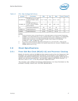
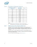
Electrical Specifications Table 18. FSB Differential Clock Specifications (800 MHz FSB) T# Parameter Min Nom Max Unit Figure Notes1 BCLK[1:0] Frequency 198.980 - 200.020 MHz - 2 T1: BCLK[1:0] Period 4.99950 - 5.00050 ns 3 3 T2: BCLK[1:0] Period Stability - - 150 ps 3 4 T5: BCLK[1:0] Rise and Fall Slew Rate 2.5 - 8 V/nS 3 5 T6: Slew Rate Matching N/A N/A 20 % 6 NOTES: 1. Unless otherwise noted, all specifications in this table apply to all processor core frequencies based on a 200 MHz BCLK[1:0]. 2. Duty Cycle (High time/Period) must be between 40 and 60%. 3. The period specified here is the average period. A given period may vary from this specification as governed by the period stability specification (T2). Min period specification is based on 300 PPM deviation from a 5 ns period. Max period specification is based on the summation of +300 PPM deviation from a 5 ns period and a +0.5% maximum variance due to spread spectrum clocking. 4. In this context, period stability is defined as the worst case timing difference between successive crossover voltages. In other words, the largest absolute difference between adjacent clock periods must be less than the period stability. 5. Measurement taken from differential waveform. 6. Matching applies to rising edge rate for Clock and falling edge rate for Clock#. It is measured using a ±75 mV window centered on the average cross point where Clock rising meets Clock# falling. The median cross point is used to calculate the voltage thresholds the oscilloscope is to use for the edge rate calculations. Slew rate matching is a single ended measurement. Figure 3. Differential Clock Waveform Threshold Region Tph BC LK 1 VCROSS (ABS) VCROSS (ABS) Ringback Margin BCLK0 Tpl Tp Tp = T1: BCLK[1:0] period T2: BCLK[1:0] period stability (not shown) Tph = T3: BCLK[1:0] pulse high time Tpl = T4: BCLK[1:0] pulse low time T5: BCLK[1:0] rise time through the threshold region T6: BCLK[1:0] fall time through the threshold region Overshoot VH Rising Edge Ringback Falling Edge Ringback VL Undershoot 30 Datasheet
-
 1
1 -
2
-
3
-
4
-
5
-
6
-
7
-
8
-
9
-
10
-
11
-
12
-
13
-
14
-
15
-
16
-
17
-
18
-
19
-
20
-
21
-
22
-
23
-
24
-
 25
25 -
 26
26 -
 27
27 -
 28
28 -
 29
29 -
 30
30 -
 31
31 -
 32
32 -
 33
33 -
 34
34 -
 35
35 -
36
-
37
-
38
-
39
-
40
-
41
-
42
-
43
-
44
-
45
-
46
-
47
-
48
-
49
-
50
-
51
-
52
-
53
-
54
-
55
-
56
-
57
-
58
-
59
-
60
-
61
-
62
-
63
-
64
-
65
-
66
-
67
-
68
-
69
-
70
-
71
-
72
-
73
-
74
-
75
-
76
-
77
-
78
-
79
-
80
-
81
-
82
-
83
-
84
-
85
-
86
-
87
-
88
-
89
-
90
-
91
-
92
-
93
-
94
-
95
-
96
-
97
-
98
-
99
-
100
 |
 |