Intel E3300 Data Sheet - Page 26
GTL+ Front Side Bus Specifications
 |
View all Intel E3300 manuals
Add to My Manuals
Save this manual to your list of manuals |
Page 26 highlights
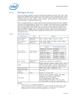
Electrical Specifications Table 13. . 2.7.3.2 PECI DC Electrical Limits Symbol Definition and Conditions Min Max Units Notes1 Vin Input Voltage Range Vhysteresis Hysteresis -0.15 VTT V 0.1 * VTT - V 2 Vn Negative-edge threshold voltage 0.275 * VTT 0.500 * VTT V Vp Positive-edge threshold voltage 0.550 * VTT 0.725 * VTT V Isource High level output source (VOH = 0.75 * VTT) -6.0 N/A mA Low level output sink Isink (VOL = 0.25 * VTT) 0.5 Ileak+ High impedance state leakage to VTT N/A 1.0 mA 50 µA 3 Ileak- High impedance leakage to GND N/A 10 µA 3 Cbus Bus capacitance per node N/A 10 pF 4 Vnoise Signal noise immunity above 300 MHz 0.1 * VTT - Vp-p NOTES: 1. VTT supplies the PECI interface. PECI behavior does not affect VTT min/max specifications. Refer to Table 4 for VTT specifications. 2. The leakage specification applies to powered devices on the PECI bus. 3. The input buffers use a Schmitt-triggered input design for improved noise immunity. 4. One node is counted for each client and one node for the system host. Extended trace lengths might appear as additional nodes. GTL+ Front Side Bus Specifications In most cases, termination resistors are not required as these are integrated into the processor silicon. See Table 8 for details on which GTL+ signals do not include on-die termination. Valid high and low levels are determined by the input buffers by comparing with a reference voltage called GTLREF. Table 14 lists the GTLREF specifications. The GTL+ reference voltage (GTLREF) should be generated on the system board using high precision voltage divider circuits. 26 Datasheet
-
 1
1 -
2
-
3
-
4
-
5
-
6
-
7
-
8
-
9
-
10
-
11
-
12
-
13
-
14
-
15
-
16
-
17
-
18
-
19
-
20
-
 21
21 -
 22
22 -
 23
23 -
 24
24 -
 25
25 -
 26
26 -
 27
27 -
 28
28 -
 29
29 -
 30
30 -
 31
31 -
32
-
33
-
34
-
35
-
36
-
37
-
38
-
39
-
40
-
41
-
42
-
43
-
44
-
45
-
46
-
47
-
48
-
49
-
50
-
51
-
52
-
53
-
54
-
55
-
56
-
57
-
58
-
59
-
60
-
61
-
62
-
63
-
64
-
65
-
66
-
67
-
68
-
69
-
70
-
71
-
72
-
73
-
74
-
75
-
76
-
77
-
78
-
79
-
80
-
81
-
82
-
83
-
84
-
85
-
86
-
87
-
88
-
89
-
90
-
91
-
92
-
93
-
94
-
95
-
96
-
97
-
98
-
99
-
100
 |
 |
