Intel E3300 Data Sheet - Page 66
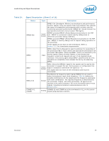
Table 24., Signal Description, Sheet 3 of 10
 |
View all Intel E3300 manuals
Add to My Manuals
Save this manual to your list of manuals |
Page 66 highlights
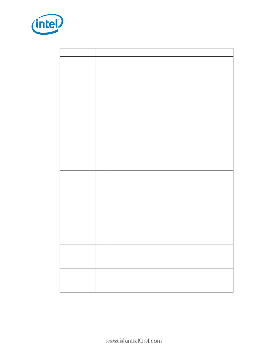
Land Listing and Signal Descriptions Table 24. Signal Description (Sheet 3 of 10) Name Type Description D[63:0]# (Data) are the data signals. These signals provide a 64bit data path between the processor FSB agents, and must connect the appropriate pins/lands on all such agents. The data driver asserts DRDY# to indicate a valid data transfer. D[63:0]# are quad-pumped signals and will, thus, be driven four times in a common clock period. D[63:0]# are latched off the falling edge of both DSTBP[3:0]# and DSTBN[3:0]#. Each group of 16 data signals correspond to a pair of one DSTBP# and one DSTBN#. The following table shows the grouping of data signals to data strobes and DBI#. D[63:0]# DBI[3:0]# DBR# DBSY# Input/ Quad-Pumped Signal Groups Output Data Group DSTBN#/DSTBP# D[15:0]# 0 D[31:16]# 1 D[47:32]# 2 D[63:48]# 3 DBI# 0 1 2 3 Furthermore, the DBI# signals determine the polarity of the data signals. Each group of 16 data signals corresponds to one DBI# signal. When the DBI# signal is active, the corresponding data group is inverted and therefore sampled active high. DBI[3:0]# (Data Bus Inversion) are source synchronous and indicate the polarity of the D[63:0]# signals.The DBI[3:0]# signals are activated when the data on the data bus is inverted. If more than half the data bits, within a 16-bit group, would have been asserted electrically low, the bus agent may invert the data bus signals for that particular sub-phase for that 16-bit group. DBI[3:0] Assignment To Data Bus Input/ Output Bus Signal Data Bus Signals DBI3# DBI2# DBI1# DBI0# D[63:48]# D[47:32]# D[31:16]# D[15:0]# Output DBR# (Debug Reset) is used only in processor systems where no debug port is implemented on the system board. DBR# is used by a debug port interposer so that an in-target probe can drive system reset. If a debug port is implemented in the system, DBR# is a no connect in the system. DBR# is not a processor signal. Input/ Output DBSY# (Data Bus Busy) is asserted by the agent responsible for driving data on the processor FSB to indicate that the data bus is in use. The data bus is released after DBSY# is de-asserted. This signal must connect the appropriate pins/lands on all processor FSB agents. 66 Datasheet
-
 1
1 -
2
-
3
-
4
-
5
-
6
-
7
-
8
-
9
-
10
-
11
-
12
-
13
-
14
-
15
-
16
-
17
-
18
-
19
-
20
-
21
-
22
-
23
-
24
-
25
-
26
-
27
-
28
-
29
-
30
-
31
-
32
-
33
-
34
-
35
-
36
-
37
-
38
-
39
-
40
-
41
-
42
-
43
-
44
-
45
-
46
-
47
-
48
-
49
-
50
-
51
-
52
-
53
-
54
-
55
-
56
-
57
-
58
-
59
-
60
-
 61
61 -
 62
62 -
 63
63 -
 64
64 -
 65
65 -
 66
66 -
 67
67 -
 68
68 -
 69
69 -
 70
70 -
 71
71 -
72
-
73
-
74
-
75
-
76
-
77
-
78
-
79
-
80
-
81
-
82
-
83
-
84
-
85
-
86
-
87
-
88
-
89
-
90
-
91
-
92
-
93
-
94
-
95
-
96
-
97
-
98
-
99
-
100
 |
 |