Intel E3300 Data Sheet - Page 19
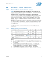
Table 5., Processor V, Static and Transient Tolerance
 |
View all Intel E3300 manuals
Add to My Manuals
Save this manual to your list of manuals |
Page 19 highlights
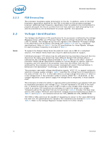
Electrical Specifications Table 5. 5. Refer to Table 5 and Figure 1, for the minimum, typical, and maximum VCC allowed for a given current. The processor should not be subjected to any VCC and ICC combination wherein VCC exceeds VCC_MAX for a given current. 6. ICC_MAX specification is based on VCC_MAX loadline. Refer to Figure 1 for details. 7. VTT must be provided using a separate voltage source and not be connected to VCC. This specification is measured at the land. 8. Baseboard bandwidth is limited to 20 MHz. 9. This is the maximum total current drawn from the VTT plane by only the processor. This specification does not include the current coming from on-board termination (RTT), through the signal line. Refer to the Voltage Regulator Design Guide to determine the total ITT drawn by the system. This parameter is based on design characterization and is not tested. 10. Adherence to the voltage specifications for the processor are required to ensure reliable processor operation. Processor VCC Static and Transient Tolerance Voltage Deviation from VID Setting (V)1, 2, 3, 4 ICC (A) Maximum Voltage 1.65 m Typical Voltage 1.73 m Minimum Voltage 1.80 m 0 0.000 -0.019 -0.038 5 -0.008 -0.028 -0.047 10 -0.017 -0.036 -0.056 15 -0.025 -0.045 -0.065 20 -0.033 -0.054 -0.074 25 -0.041 -0.062 -0.083 30 -0.050 -0.071 -0.092 35 -0.058 -0.079 -0.101 40 -0.066 -0.088 -0.110 45 -0.074 -0.097 -0.119 50 -0.083 -0.105 -0.128 55 -0.091 -0.114 -0.137 60 -0.099 -0.123 -0.146 65 -0.107 -0.131 -0.155 70 -0.116 -0.140 -0.164 75 -0.124 -0.148 -0.173 NOTES: 1. The loadline specification includes both static and transient limits except for overshoot allowed as shown in Section 2.6.3. 2. This table is intended to aid in reading discrete points on Figure 1. 3. The loadlines specify voltage limits at the die measured at the VCC_SENSE and VSS_SENSE lands. Voltage regulation feedback for voltage regulator circuits must be taken from processor VCC and VSS lands. Refer to the Voltage Regulator Design Guide for socket loadline guidelines and VR implementation details. 4. Adherence to this loadline specification is required to ensure reliable processor operation. Datasheet 19
-
 1
1 -
2
-
3
-
4
-
5
-
6
-
7
-
8
-
9
-
10
-
11
-
12
-
13
-
 14
14 -
 15
15 -
 16
16 -
 17
17 -
 18
18 -
 19
19 -
 20
20 -
 21
21 -
 22
22 -
 23
23 -
 24
24 -
25
-
26
-
27
-
28
-
29
-
30
-
31
-
32
-
33
-
34
-
35
-
36
-
37
-
38
-
39
-
40
-
41
-
42
-
43
-
44
-
45
-
46
-
47
-
48
-
49
-
50
-
51
-
52
-
53
-
54
-
55
-
56
-
57
-
58
-
59
-
60
-
61
-
62
-
63
-
64
-
65
-
66
-
67
-
68
-
69
-
70
-
71
-
72
-
73
-
74
-
75
-
76
-
77
-
78
-
79
-
80
-
81
-
82
-
83
-
84
-
85
-
86
-
87
-
88
-
89
-
90
-
91
-
92
-
93
-
94
-
95
-
96
-
97
-
98
-
99
-
100
 |
 |