Intel E3300 Data Sheet - Page 56
Power/Other
 |
View all Intel E3300 manuals
Add to My Manuals
Save this manual to your list of manuals |
Page 56 highlights
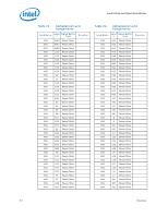
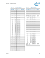
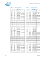
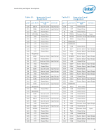
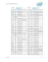
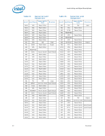
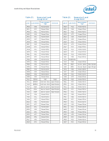
Land Listing and Signal Descriptions Table 23. Numerical Land Assignment Land # Land Name Signal Buffer Type Direction F11 D23# Source Synch Input/Output F12 D24# Source Synch Input/Output F13 VSS Power/Other F14 D28# Source Synch Input/Output F15 D30# Source Synch Input/Output F16 VSS Power/Other F17 D37# Source Synch Input/Output F18 D38# Source Synch Input/Output F19 VSS Power/Other F20 D41# Source Synch Input/Output F21 D43# Source Synch Input/Output F22 VSS Power/Other F23 RESERVED F24 TESTHI7 Power/Other Input F25 TESTHI2 Power/Other Input F26 TESTHI0 Power/Other Input F27 VTT_SEL Power/Other Output F28 BCLK0 Clock Input F29 RESERVED G1 FC27 Power/Other G2 COMP2 Power/Other Input G3 TESTHI8/ FC42 Power/Other Input G4 TESTHI9/ FC43 Power/Other Input G5 PECI Power/Other Input/Output G6 RESERVED G7 DEFER# Common Clock Input G8 G9 G10 G11 G12 G13 G14 G15 G16 BPRI# D16# FC38 DBI1# DSTBN1# D27# D29# D31# D32# Common Clock Input Source Synch Input/Output Power/Other Source Synch Input/Output Source Synch Input/Output Source Synch Input/Output Source Synch Input/Output Source Synch Input/Output Source Synch Input/Output G17 G18 G19 D36# D35# DSTBP2# Source Synch Input/Output Source Synch Input/Output Source Synch Input/Output Table 23. Numerical Land Assignment Land # Land Name Signal Buffer Type Direction G20 DSTBN2# Source Synch Input/Output G21 G22 G23 D44# D47# RESET# Source Synch Input/Output Source Synch Input/Output Common Clock Input G24 G25 G26 G27 G28 G29 G30 H1 H2 TESTHI6 TESTHI3 TESTHI5 TESTHI4 BCLK1 BSEL0 BSEL2 GTLREF0 GTLREF1 Power/Other Power/Other Power/Other Power/Other Clock Asynch CMOS Asynch CMOS Power/Other Power/Other Input Input Input Input Input Output Output Input Input H3 H4 H5 H6 H7 H8 H9 H10 H11 VSS FC35 TESTHI10 VSS VSS VSS VSS VSS VSS Power/Other Power/Other Power/Other Power/Other Power/Other Power/Other Power/Other Power/Other Power/Other Input H12 H13 H14 VSS VSS VSS Power/Other Power/Other Power/Other H15 H16 H17 H18 H19 H20 FC32 FC33 VSS VSS VSS VSS Power/Other Power/Other Power/Other Power/Other Power/Other Power/Other H21 H22 H23 VSS VSS VSS Power/Other Power/Other Power/Other H24 H25 H26 H27 H28 VSS VSS VSS VSS VSS Power/Other Power/Other Power/Other Power/Other Power/Other 56 Datasheet
-
 1
1 -
2
-
3
-
4
-
5
-
6
-
7
-
8
-
9
-
10
-
11
-
12
-
13
-
14
-
15
-
16
-
17
-
18
-
19
-
20
-
21
-
22
-
23
-
24
-
25
-
26
-
27
-
28
-
29
-
30
-
31
-
32
-
33
-
34
-
35
-
36
-
37
-
38
-
39
-
40
-
41
-
42
-
43
-
44
-
45
-
46
-
47
-
48
-
49
-
50
-
 51
51 -
 52
52 -
 53
53 -
 54
54 -
 55
55 -
 56
56 -
 57
57 -
 58
58 -
 59
59 -
 60
60 -
 61
61 -
62
-
63
-
64
-
65
-
66
-
67
-
68
-
69
-
70
-
71
-
72
-
73
-
74
-
75
-
76
-
77
-
78
-
79
-
80
-
81
-
82
-
83
-
84
-
85
-
86
-
87
-
88
-
89
-
90
-
91
-
92
-
93
-
94
-
95
-
96
-
97
-
98
-
99
-
100
 |
 |