Intel E3300 Data Sheet - Page 64
Alphabetical Signals Reference - 64 bit
 |
View all Intel E3300 manuals
Add to My Manuals
Save this manual to your list of manuals |
Page 64 highlights
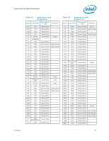
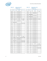
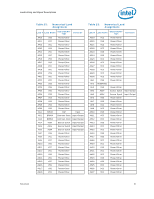
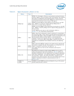
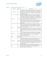
Land Listing and Signal Descriptions 4.2 Alphabetical Signals Reference Table 24. Signal Description (Sheet 1 of 10) Name A[35:3]# A20M# ADS# ADSTB[1:0]# Type Description Input/ Output A[35:3]# (Address) define a 236-byte physical memory address space. In sub-phase 1 of the address phase, these signals transmit the address of a transaction. In sub-phase 2, these signals transmit transaction type information. These signals must connect the appropriate pins/lands of all agents on the processor FSB. A[35:3]# are source synchronous signals and are latched into the receiving buffers by ADSTB[1:0]#. On the active-to-inactive transition of RESET#, the processor samples a subset of the A[35:3]# signals to determine power-on configuration. See Section 6.1 for more details. Input If A20M# (Address-20 Mask) is asserted, the processor masks physical address bit 20 (A20#) before looking up a line in any internal cache and before driving a read/write transaction on the bus. Asserting A20M# emulates the 8086 processor's address wrap-around at the 1-MB boundary. Assertion of A20M# is only supported in real mode. A20M# is an asynchronous signal. However, to ensure recognition of this signal following an Input/Output write instruction, it must be valid along with the TRDY# assertion of the corresponding Input/ Output Write bus transaction. Input/ Output ADS# (Address Strobe) is asserted to indicate the validity of the transaction address on the A[35:3]# and REQ[4:0]# signals. All bus agents observe the ADS# activation to begin protocol checking, address decode, internal snoop, or deferred reply ID match operations associated with the new transaction. Address strobes are used to latch A[35:3]# and REQ[4:0]# on their rising and falling edges. Strobes are associated with signals as shown below. Input/ Output Signals REQ[4:0]#, A[16:3]# Associated Strobe ADSTB0# A[35:17]# ADSTB1# BCLK[1:0] BNR# Input The differential pair BCLK (Bus Clock) determines the FSB frequency. All processor FSB agents must receive these signals to drive their outputs and latch their inputs. All external timing parameters are specified with respect to the rising edge of BCLK0 crossing VCROSS. Input/ Output BNR# (Block Next Request) is used to assert a bus stall by any bus agent unable to accept new bus transactions. During a bus stall, the current bus owner cannot issue any new transactions. 64 Datasheet
-
 1
1 -
2
-
3
-
4
-
5
-
6
-
7
-
8
-
9
-
10
-
11
-
12
-
13
-
14
-
15
-
16
-
17
-
18
-
19
-
20
-
21
-
22
-
23
-
24
-
25
-
26
-
27
-
28
-
29
-
30
-
31
-
32
-
33
-
34
-
35
-
36
-
37
-
38
-
39
-
40
-
41
-
42
-
43
-
44
-
45
-
46
-
47
-
48
-
49
-
50
-
51
-
52
-
53
-
54
-
55
-
56
-
57
-
58
-
 59
59 -
 60
60 -
 61
61 -
 62
62 -
 63
63 -
 64
64 -
 65
65 -
 66
66 -
 67
67 -
 68
68 -
 69
69 -
70
-
71
-
72
-
73
-
74
-
75
-
76
-
77
-
78
-
79
-
80
-
81
-
82
-
83
-
84
-
85
-
86
-
87
-
88
-
89
-
90
-
91
-
92
-
93
-
94
-
95
-
96
-
97
-
98
-
99
-
100
 |
 |