Intel E3300 Data Sheet - Page 70
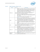
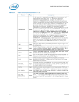
Table 24., Signal Description, Sheet 7 of 10
 |
View all Intel E3300 manuals
Add to My Manuals
Save this manual to your list of manuals |
Page 70 highlights
Land Listing and Signal Descriptions Table 24. Signal Description (Sheet 7 of 10) Name Type Description PWRGOOD REQ[4:0]# RESET# RESERVED RS[2:0]# SKTOCC# Input PWRGOOD (Power Good) is a processor input. The processor requires this signal to be a clean indication that the clocks and power supplies are stable and within their specifications. 'Clean' implies that the signal will remain low (capable of sinking leakage current), without glitches, from the time that the power supplies are turned on until they come within specification. The signal must then transition monotonically to a high state. PWRGOOD can be driven inactive at any time, but clocks and power must again be stable before a subsequent rising edge of PWRGOOD. The PWRGOOD signal must be supplied to the processor; it is used to protect internal circuits against voltage sequencing issues. It should be driven high throughout boundary scan operation. Input/ Output REQ[4:0]# (Request Command) must connect the appropriate pins/lands of all processor FSB agents. They are asserted by the current bus owner to define the currently active transaction type. These signals are source synchronous to ADSTB0#. Input Asserting the RESET# signal resets the processor to a known state and invalidates its internal caches without writing back any of their contents. For a power-on Reset, RESET# must stay active for at least one millisecond after VCC and BCLK have reached their proper specifications. On observing active RESET#, all FSB agents will deassert their outputs within two clocks. RESET# must not be kept asserted for more than 10 ms while PWRGOOD is asserted. A number of bus signals are sampled at the active-to-inactive transition of RESET# for power-on configuration. These configuration options are described in the Section 6.1. This signal does not have on-die termination and must be terminated on the system board. All RESERVED lands must remain unconnected. Connection of these lands to VCC, VSS, VTT, or to any other signal (including each other) can result in component malfunction or incompatibility with future processors. Input RS[2:0]# (Response Status) are driven by the response agent (the agent responsible for completion of the current transaction), and must connect the appropriate pins/lands of all processor FSB agents. SKTOCC# (Socket Occupied) will be pulled to ground by the Output processor. System board designers may use this signal to determine if the processor is present. 70 Datasheet
-
 1
1 -
2
-
3
-
4
-
5
-
6
-
7
-
8
-
9
-
10
-
11
-
12
-
13
-
14
-
15
-
16
-
17
-
18
-
19
-
20
-
21
-
22
-
23
-
24
-
25
-
26
-
27
-
28
-
29
-
30
-
31
-
32
-
33
-
34
-
35
-
36
-
37
-
38
-
39
-
40
-
41
-
42
-
43
-
44
-
45
-
46
-
47
-
48
-
49
-
50
-
51
-
52
-
53
-
54
-
55
-
56
-
57
-
58
-
59
-
60
-
61
-
62
-
63
-
64
-
 65
65 -
 66
66 -
 67
67 -
 68
68 -
 69
69 -
 70
70 -
 71
71 -
 72
72 -
 73
73 -
 74
74 -
 75
75 -
76
-
77
-
78
-
79
-
80
-
81
-
82
-
83
-
84
-
85
-
86
-
87
-
88
-
89
-
90
-
91
-
92
-
93
-
94
-
95
-
96
-
97
-
98
-
99
-
100
 |
 |