Intel E3300 Data Sheet - Page 71
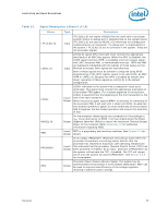
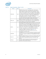
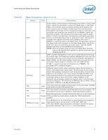
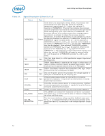
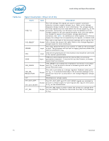
Table 24., Signal Description, Sheet 8 of 10
 |
View all Intel E3300 manuals
Add to My Manuals
Save this manual to your list of manuals |
Page 71 highlights
Land Listing and Signal Descriptions Table 24. Signal Description (Sheet 8 of 10) Name Type Description SLP# SMI# STPCLK# TCK TDI Input Input Input Input Input SLP# (Sleep), when asserted in Extended Stop Grant or Stop Grant state, causes the processor to enter the Sleep state. In the Sleep state, the processor stops providing internal clock signals to all units, leaving only the Phase-Locked Loop (PLL) still operating. Processors in this state will not recognize snoops or interrupts. The processor will recognize only assertion of the RESET# signal, deassertion of SLP#, and removal of the BCLK input while in Sleep state. If SLP# is de-asserted, the processor exits Sleep state and returns to Extended Stop Grant or Stop Grant state, restarting its internal clock signals to the bus and processor core units. If DPSLP# is asserted while in the Sleep state, the processor will exit the Sleep state and transition to the Deep Sleep state. Use of the SLP# pin, and corresponding low power state, requires chipset support and may not be available on all platforms. NOTE: Some processors may not have the Sleep State enabled, refer to the Specification Update for specific processor and stepping guidance. SMI# (System Management Interrupt) is asserted asynchronously by system logic. On accepting a System Management Interrupt, the processor saves the current state and enter System Management Mode (SMM). An SMI Acknowledge transaction is issued, and the processor begins program execution from the SMM handler. If SMI# is asserted during the de-assertion of RESET#, the processor will tri-state its outputs. STPCLK# (Stop Clock), when asserted, causes the processor to enter a low power Stop-Grant state. The processor issues a StopGrant Acknowledge transaction, and stops providing internal clock signals to all processor core units except the FSB and APIC units. The processor continues to snoop bus transactions and service interrupts while in Stop-Grant state. When STPCLK# is deasserted, the processor restarts its internal clock to all units and resumes execution. The assertion of STPCLK# has no effect on the bus clock; STPCLK# is an asynchronous input. TCK (Test Clock) provides the clock input for the processor Test Bus (also known as the Test Access Port). TDI (Test Data In) transfers serial test data into the processor. TDI provides the serial input needed for JTAG specification support. TDO TESTHI[12,10:0] TDO (Test Data Out) transfers serial test data out of the processor. Output TDO provides the serial output needed for JTAG specification support. Input The TESTHI[12,10:0] lands must be connected to the processor's appropriate power source (refer to VTT_OUT_LEFT and VTT_OUT_RIGHT signal description) through a resistor for proper processor operation. See Section 2.4 for more details. Datasheet 71
-
 1
1 -
2
-
3
-
4
-
5
-
6
-
7
-
8
-
9
-
10
-
11
-
12
-
13
-
14
-
15
-
16
-
17
-
18
-
19
-
20
-
21
-
22
-
23
-
24
-
25
-
26
-
27
-
28
-
29
-
30
-
31
-
32
-
33
-
34
-
35
-
36
-
37
-
38
-
39
-
40
-
41
-
42
-
43
-
44
-
45
-
46
-
47
-
48
-
49
-
50
-
51
-
52
-
53
-
54
-
55
-
56
-
57
-
58
-
59
-
60
-
61
-
62
-
63
-
64
-
65
-
 66
66 -
 67
67 -
 68
68 -
 69
69 -
 70
70 -
 71
71 -
 72
72 -
 73
73 -
 74
74 -
 75
75 -
 76
76 -
77
-
78
-
79
-
80
-
81
-
82
-
83
-
84
-
85
-
86
-
87
-
88
-
89
-
90
-
91
-
92
-
93
-
94
-
95
-
96
-
97
-
98
-
99
-
100
 |
 |