Intel E3300 Data Sheet - Page 55
Datasheet, Source Synch, Input/Output, Power/Other, VCCIOPLL, RESERVED, Common Clock, VCCPLL, Input
 |
View all Intel E3300 manuals
Add to My Manuals
Save this manual to your list of manuals |
Page 55 highlights
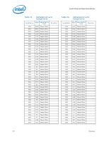
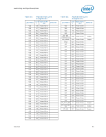
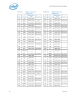
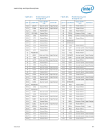
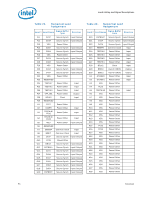
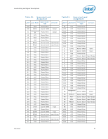
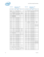
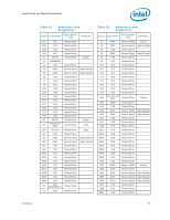
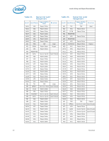
Land Listing and Signal Descriptions Table 23. Numerical Land Assignment Land # Land Name Signal Buffer Type Direction C20 C21 C22 C23 C24 C25 C26 C27 C28 C29 C30 D1 D2 D3 D4 D5 D6 D7 D8 D9 D10 D11 D12 D13 D14 D15 D16 D17 D18 D19 D20 D21 D22 D23 D24 D25 D26 D27 D28 DBI3# Source Synch Input/Output D58# Source Synch Input/Output VSS Power/Other VCCIOPLL Power/Other VSS Power/Other VTT Power/Other VTT Power/Other VTT Power/Other VTT Power/Other VTT Power/Other VTT Power/Other RESERVED ADS# Common Clock Input/Output VSS Power/Other HIT# Common Clock Input/Output VSS Power/Other VSS Power/Other D20# Source Synch Input/Output D12# Source Synch Input/Output VSS Power/Other D22# Source Synch Input/Output D15# Source Synch Input/Output VSS Power/Other D25# Source Synch Input/Output RESERVED VSS Power/Other RESERVED D49# Source Synch Input/Output VSS Power/Other DBI2# Source Synch Input/Output D48# Source Synch Input/Output VSS Power/Other D46# Source Synch Input/Output VCCPLL Power/Other VSS Power/Other VTT Power/Other VTT Power/Other VTT Power/Other VTT Power/Other Table 23. Numerical Land Assignment Land # Land Name Signal Buffer Type Direction D29 D30 E2 E3 E4 E5 E6 E7 E8 E9 E10 E11 E12 E13 E14 E15 E16 E17 E18 E19 E20 E21 E22 E23 E24 E25 E26 E27 E28 E29 F2 F3 F4 F5 F6 F7 F8 F9 F10 VTT Power/Other VTT Power/Other VSS Power/Other TRDY# Common Clock Input HITM# Common Clock Input/Output FC20 Power/Other RESERVED RESERVED VSS Power/Other D19# Source Synch Input/Output D21# Source Synch Input/Output VSS Power/Other DSTBP1# Source Synch Input/Output D26# Source Synch Input/Output VSS Power/Other D33# Source Synch Input/Output D34# Source Synch Input/Output VSS Power/Other D39# Source Synch Input/Output D40# Source Synch Input/Output VSS Power/Other D42# Source Synch Input/Output D45# Source Synch Input/Output RESERVED FC10 Power/Other VSS Power/Other VSS Power/Other VSS Power/Other VSS Power/Other FC26 Power/Other FC5 Power/Other BR0# Common Clock Input/Output VSS Power/Other RS1# Common Clock Input FC21 Power/Other VSS Power/Other D17# Source Synch Input/Output D18# Source Synch Input/Output VSS Power/Other Datasheet 55
-
 1
1 -
2
-
3
-
4
-
5
-
6
-
7
-
8
-
9
-
10
-
11
-
12
-
13
-
14
-
15
-
16
-
17
-
18
-
19
-
20
-
21
-
22
-
23
-
24
-
25
-
26
-
27
-
28
-
29
-
30
-
31
-
32
-
33
-
34
-
35
-
36
-
37
-
38
-
39
-
40
-
41
-
42
-
43
-
44
-
45
-
46
-
47
-
48
-
49
-
 50
50 -
 51
51 -
 52
52 -
 53
53 -
 54
54 -
 55
55 -
 56
56 -
 57
57 -
 58
58 -
 59
59 -
 60
60 -
61
-
62
-
63
-
64
-
65
-
66
-
67
-
68
-
69
-
70
-
71
-
72
-
73
-
74
-
75
-
76
-
77
-
78
-
79
-
80
-
81
-
82
-
83
-
84
-
85
-
86
-
87
-
88
-
89
-
90
-
91
-
92
-
93
-
94
-
95
-
96
-
97
-
98
-
99
-
100
 |
 |