SanDisk SDCFH-004G Product Manual - Page 26
Electrical Specification
 |
UPC - 878587001044
View all SanDisk SDCFH-004G manuals
Add to My Manuals
Save this manual to your list of manuals |
Page 26 highlights
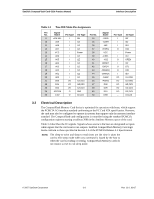
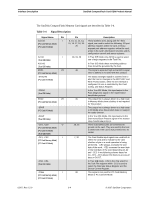
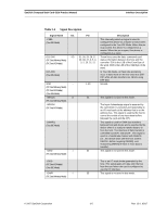
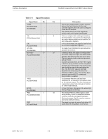
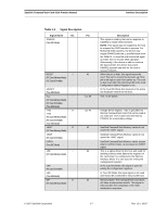
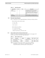
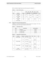
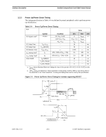
Interface Description SanDisk CompactFlash Card OEM Product Manual Table 3-4 Signal Description Signal Name Dir. Pin -IOIS16 (PC Card I/O Mode) -IOCS16 (True IDE Mode) Description I/O Operation-When the card is configured for I/O Operation, pin 24 is used for the -I/O Selected is 16 Bit Port (-IOIS16) function. A low signal indicates that a 16-bit or odd-byte only operation can be performed at the addressed port. This output signal is asserted low when this device is expecting a word data transfer cycle. 3.3 Electrical Specification All D.C. Characteristics for the CompactFlash Memory Card Series are defined as follows: Typical conditions unless otherwise stated: VCC = 5V +/- 10% VCC = 3.3V +/- 5% Ta = 0 ° C to 60 ° C Absolute Maximum conditions: VCC = -0.3V min. to 6.5V max. V* = 0.5V min. to VCC + 0.5V max. *Voltage on any pin except VCC with respect to GND. 3.3.1 Input Leakage Control and Input Characteristics In Table 3-5, "x" refers to the characteristics described in Table 3-6. For example-"I1U" indicates a pull-up resistor with a Type 1 input characteristic. Table 3-5 Input Leakage Control Type lxZ IxU IxD Parameter Input Leakage Current Pull Up Resistor Pull Down Resistor Symbol IL RPU1 RPD1 Conditions Vih=VCC/Vil=GND VCC=5.0V VCC=5.0V MIN MAX Unit -1 1 uA 50k 500k Ohm 50k 500k Ohm NOTE: The minimum pull-up resistor leakage current meets the PCMCIA specification of 10k ohms but is intentionally higher in the CompactFlash Memory Card Series product to reduce power use. 02/07, Rev. 12.0 3-8 © 2007 SanDisk Corporation
-
 1
1 -
2
-
3
-
4
-
5
-
6
-
7
-
8
-
9
-
10
-
11
-
12
-
13
-
14
-
15
-
16
-
17
-
18
-
19
-
20
-
 21
21 -
 22
22 -
 23
23 -
 24
24 -
 25
25 -
 26
26 -
 27
27 -
 28
28 -
 29
29 -
 30
30 -
 31
31 -
32
-
33
-
34
-
35
-
36
-
37
-
38
-
39
-
40
-
41
-
42
-
43
-
44
-
45
-
46
-
47
-
48
-
49
-
50
-
51
-
52
-
53
-
54
-
55
-
56
-
57
-
58
-
59
-
60
-
61
-
62
-
63
-
64
-
65
-
66
-
67
-
68
-
69
-
70
-
71
-
72
-
73
-
74
-
75
-
76
-
77
-
78
-
79
-
80
-
81
-
82
-
83
-
84
-
85
-
86
-
87
-
88
-
89
-
90
-
91
-
92
-
93
-
94
-
95
-
96
-
97
-
98
-
99
-
100
-
101
-
102
-
103
-
104
-
105
-
106
-
107
-
108
 |
 |