SanDisk SDCFH-004G Product Manual - Page 34
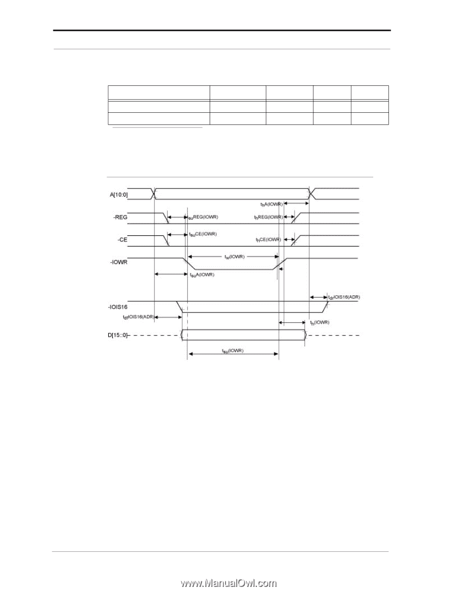
Table 3-13, I/O Read Input Timing Specification, I/O Write Timing Diagram
 |
UPC - 878587001044
View all SanDisk SDCFH-004G manuals
Add to My Manuals
Save this manual to your list of manuals |
Page 34 highlights
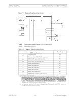
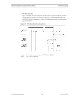
Interface Description SanDisk CompactFlash Card OEM Product Manual Table 3-13 I/O Read (Input) Timing Specification Item -IOIS16 Delay falling from Address -IOIS16 Delay rising from Address Symbol tdfIOIS16(ADR) tdrIOIS16(ADR) IEEE Symbol tAVISL tAVISH Min. (ns) ----- a. The maximum load on -INPACK and -IOIS16 is 1 LSTTL with 50 pF total load. Max. (ns) 35a 35a 3.3.9 I/O Write (Output) Timing Specification Figure 3-6 I/O Write Timing Diagram NOTE 1: NOTE 2: NOTE 3: All timings are measured at the CompactFlash Memory Card. Skews and delays from the host system driver/receiver to the CompactFlash Memory Card must be accounted for by the system design. D[15::0] signifies data provided by the host system to the CompactFlash Memory Card. 02/07, Rev. 12.0 3-16 © 2007 SanDisk Corporation
-
 1
1 -
2
-
3
-
4
-
5
-
6
-
7
-
8
-
9
-
10
-
11
-
12
-
13
-
14
-
15
-
16
-
17
-
18
-
19
-
20
-
21
-
22
-
23
-
24
-
25
-
26
-
27
-
28
-
 29
29 -
 30
30 -
 31
31 -
 32
32 -
 33
33 -
 34
34 -
 35
35 -
 36
36 -
 37
37 -
 38
38 -
 39
39 -
40
-
41
-
42
-
43
-
44
-
45
-
46
-
47
-
48
-
49
-
50
-
51
-
52
-
53
-
54
-
55
-
56
-
57
-
58
-
59
-
60
-
61
-
62
-
63
-
64
-
65
-
66
-
67
-
68
-
69
-
70
-
71
-
72
-
73
-
74
-
75
-
76
-
77
-
78
-
79
-
80
-
81
-
82
-
83
-
84
-
85
-
86
-
87
-
88
-
89
-
90
-
91
-
92
-
93
-
94
-
95
-
96
-
97
-
98
-
99
-
100
-
101
-
102
-
103
-
104
-
105
-
106
-
107
-
108
 |
 |