SanDisk SDCFH-004G Product Manual - Page 40
Table 3-18, Configuration Registers Decoding, Table 3-19, Attribute Memory Function
 |
UPC - 878587001044
View all SanDisk SDCFH-004G manuals
Add to My Manuals
Save this manual to your list of manuals |
Page 40 highlights
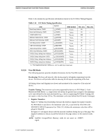
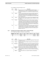
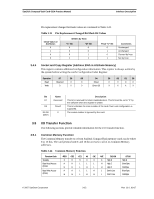
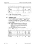
Interface Description SanDisk CompactFlash Card OEM Product Manual Decoding for the configuration registers is defined in Table 3-18. Table 3-18 Configuration Registers Decoding A8-CE2 -CE1 -REG -OE -WE A10 A9 A4 A3 A2 A1 A0 Selected Register X 0 0 0 1 0 1 00 0 0 0 0 Configuration Option Read X 0 0 1 0 0 1 00 0 0 0 0 Configuration Option Write X 0 0 0 1 0 1 00 0 0 1 0 Card Status Read X 0 0 1 0 0 1 00 0 0 1 0 Card Status Write X 0 0 0 1 0 1 00 0 1 0 0 Pin Replacement Read X 0 0 1 0 0 1 00 0 1 0 0 Pin Replacement Write X 0 0 0 1 0 1 00 0 1 1 0 Socket and Copy Read X 0 0 1 0 0 1 00 0 1 1 0 Socket and Copy Write 3.4.1 Attribute Memory Function Attribute Memory is a space where a CompactFlash Memory Card identification and configuration information is stored, and is limited to 8-bit wide accesses only at even addresses. The card configuration registers are also located there. For the Attribute Memory Read function, signals -REG and -OE must be active and -WE inactive during the cycle. As in the Main Memory Read functions, the signals -CE1 and -CE2 control the even-byte and odd-byte address, but only the even-byte data is valid during the Attribute Memory access. Refer to Table 3-19 for signal states and bus validity for the Attribute Memory function. NOTE: The -CE signal or both the -OE and -WE signal must be de-asserted between consecutive cycle operaitons. Table 3-19 Attribute Memory Function Function Mode -REG -CE2 -CE1 A9 A0 -OE -WE D15-D8 D7-D0 Standby X H H X X X X High Z High Z Read Byte Access CIS ROM L H L L L L H High Z Even (8 bits) Byte Write Byte Access CIS (8 bits) L H L L L H L Don't Even (Invalid) Care Byte Read Byte Access Configuration (8 bits) L H L H L L H High Z Even Byte Write Byte Access Configuration (8 bits) L H L H L H L Don't Even Care Byte Read Word Access CIS (16 bits) L L L L X L H Not Valid Even Byte Write Word Access CIS (16 bits) (Invalid) L L L L X H L Don't Even Care Byte Read Word Access Configuration (16 bits) L L L H X L H Not Valid Even Byte Write Word Access Configuration (16 bits) L L L H X H L Don't Even Care Byte 02/07, Rev. 12.0 3-22 © 2007 SanDisk Corporation
-
 1
1 -
2
-
3
-
4
-
5
-
6
-
7
-
8
-
9
-
10
-
11
-
12
-
13
-
14
-
15
-
16
-
17
-
18
-
19
-
20
-
21
-
22
-
23
-
24
-
25
-
26
-
27
-
28
-
29
-
30
-
31
-
32
-
33
-
34
-
 35
35 -
 36
36 -
 37
37 -
 38
38 -
 39
39 -
 40
40 -
 41
41 -
 42
42 -
 43
43 -
 44
44 -
 45
45 -
46
-
47
-
48
-
49
-
50
-
51
-
52
-
53
-
54
-
55
-
56
-
57
-
58
-
59
-
60
-
61
-
62
-
63
-
64
-
65
-
66
-
67
-
68
-
69
-
70
-
71
-
72
-
73
-
74
-
75
-
76
-
77
-
78
-
79
-
80
-
81
-
82
-
83
-
84
-
85
-
86
-
87
-
88
-
89
-
90
-
91
-
92
-
93
-
94
-
95
-
96
-
97
-
98
-
99
-
100
-
101
-
102
-
103
-
104
-
105
-
106
-
107
-
108
 |
 |
