SanDisk SDCFH-004G Product Manual - Page 47
Memory Mapped Addressing
 |
UPC - 878587001044
View all SanDisk SDCFH-004G manuals
Add to My Manuals
Save this manual to your list of manuals |
Page 47 highlights
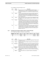
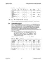
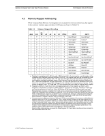
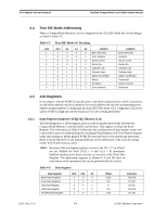
SanDisk CompactFlash Card OEM Product Manual ATA Register Set and Protocol 4.3 Memory Mapped Addressing When CompactFlash Memory Card registers are accessed via memory references, they appear in the common memory space window: 0-2K bytes as shown in Table 4-4. Table 4-4 Memory Mapped Decoding A9-REG A10 A4 A3 A2 A1 A0 Offset -OE=0 -WE=0 1 0 X 0 0 0 0 0 Even RD Dataa Even WR Dataa 1 0 X 0 0 0 1 1 Error Registerb Featuresb 1 0 X 0 0 1 0 2 Sector Count Sector Count 1 0 X 0 0 1 1 3 Sector No. Sector No. 1 0 X 0 1 0 0 4 Cylinder Low Cylinder Low 1 0 X 0 1 0 1 5 Cylinder High Cylinder High 1 0 X 0 1 1 0 6 Select Card/Head Select Card/Head 1 0 X 0 1 1 1 7 Status Command 1 0 X 1 0 0 0 8 Dup Even RD Datab Dup Even WR Datab 1 0 X 1 0 0 1 9 Dup Odd RD Datab Dup Odd WR Datab 1 0 X 1 1 0 1 D Dup Errorb Dup Featuresb 1 0 X 1 1 1 0 E Alt Status Device Ctl 1 0 X 1 1 1 1 F Drive Address Reserved 1 1 X X X X 0 8 Even RD Datac Even WR Datac 1 1 X X X X 1 9 Odd RD Datac Even RD Datac a. Register 0 is accessed with -CE1 low and -CE2 low (and A0 = Do not care) as a word register on the combined Odd Data Bus and Even Data Bus (D15-D0). This register may also be accessed by a pair of byte accesses to the offset 0 with -CE1 low and -CE2 high. Note that the address space of this word register overlaps the address space of the Error and Feature byte-wide registers that lie at off set 1. When accessed twice as byte register with CE1 low, the first byte to be accessed is the even byte of the word and the second byte accessed is the odd byte of the equivalent word access. A byte access to register 0 with CE1 high and CE2 low accesses the error (read) or feature (write) register. b. Registers at offset 8, 9 and D are non-overlapping duplicates of the registers at offset 0 and 1. Register 8 is equivalent to register 0, while register 9 accesses the odd byte. Therefore, if the regis ters are byte accessed in the order 9 then 8 the data will be transferred odd byte then even byte. Repeated byte accesses to register 8 or 0 will access consecutive (even than odd) bytes from the data buffer. Repeated word accesses to register 8, 9 or 0 will access consecutive words from the data buffer. Repeated byte accesses to register 9 are not supported. However, repeated alternating byte accesses to registers 8 then 9 will access consecutive (even then odd) bytes from the data buffer. Byte accesses to register 9 access only the odd byte of the data. c. Accesses to even addresses between 400h and 7FFh access register 8. Accesses to odd addresses between 400h and 7FFh access register 9. This 1 KByte memory window to the data register is pro vided so that hosts can perform memory to memory block moves to the data register when the regis ter lies in memory space. Some hosts, such as the X86 processors, must increment both the source and destination addresses when executing the memory to memory block move instruction. Some PCMCIA socket adapters also have auto incrementing address logic embedded within them. This address window allows these hosts and adapters to function efficiently. Note that this entire window accesses the Data Register FIFO and does not allow random access to the data buffer within the card. © 2007 SanDisk Corporation 4-3 Rev. 12.0, 02/07
-
 1
1 -
2
-
3
-
4
-
5
-
6
-
7
-
8
-
9
-
10
-
11
-
12
-
13
-
14
-
15
-
16
-
17
-
18
-
19
-
20
-
21
-
22
-
23
-
24
-
25
-
26
-
27
-
28
-
29
-
30
-
31
-
32
-
33
-
34
-
35
-
36
-
37
-
38
-
39
-
40
-
41
-
 42
42 -
 43
43 -
 44
44 -
 45
45 -
 46
46 -
 47
47 -
 48
48 -
 49
49 -
 50
50 -
 51
51 -
 52
52 -
53
-
54
-
55
-
56
-
57
-
58
-
59
-
60
-
61
-
62
-
63
-
64
-
65
-
66
-
67
-
68
-
69
-
70
-
71
-
72
-
73
-
74
-
75
-
76
-
77
-
78
-
79
-
80
-
81
-
82
-
83
-
84
-
85
-
86
-
87
-
88
-
89
-
90
-
91
-
92
-
93
-
94
-
95
-
96
-
97
-
98
-
99
-
100
-
101
-
102
-
103
-
104
-
105
-
106
-
107
-
108
 |
 |