SanDisk SDCFH-004G Product Manual - Page 53
Card Drive Address Register con't
 |
UPC - 878587001044
View all SanDisk SDCFH-004G manuals
Add to My Manuals
Save this manual to your list of manuals |
Page 53 highlights
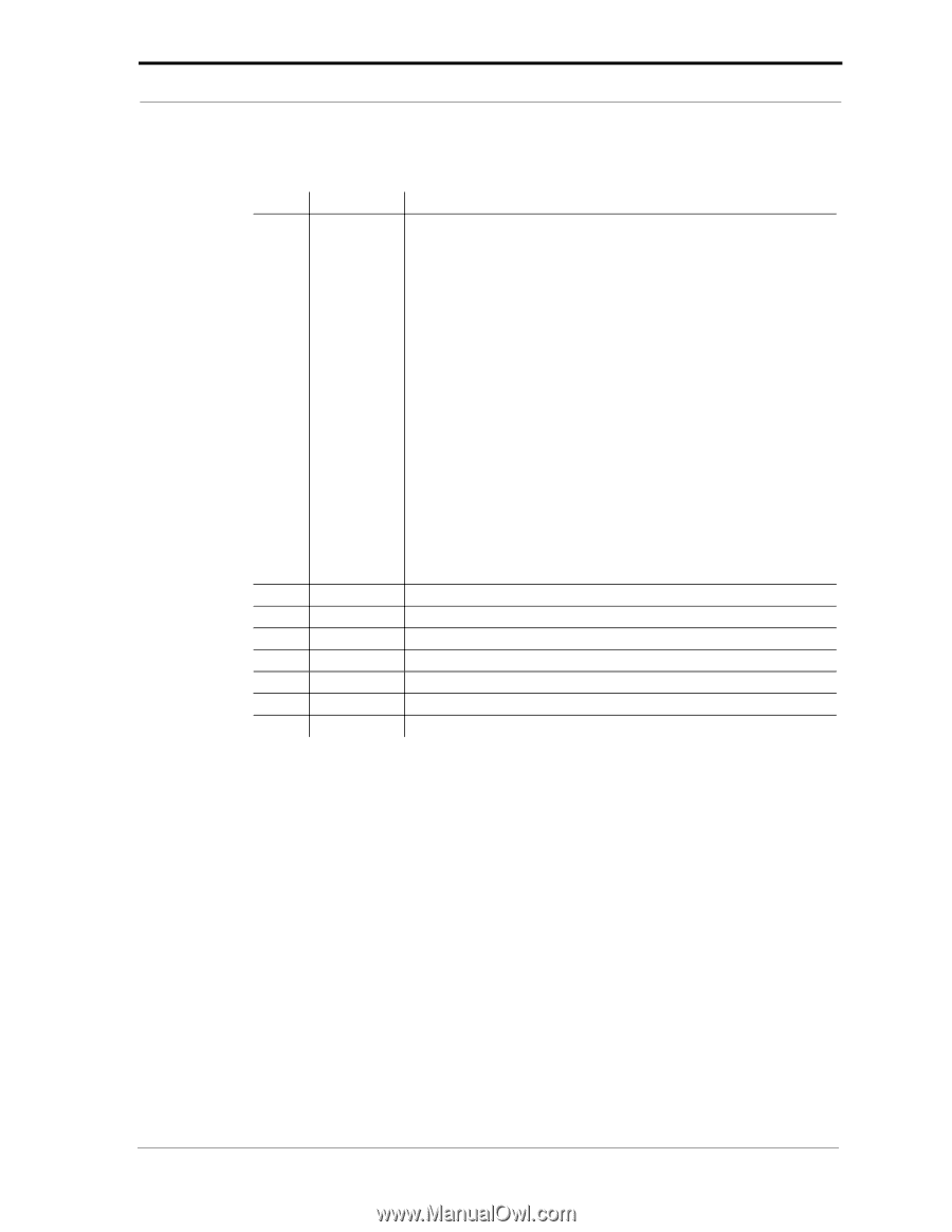
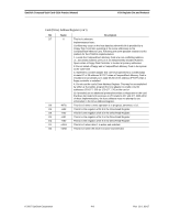
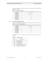
SanDisk CompactFlash Card OEM Product Manual ATA Register Set and Protocol Card (Drive) Address Register (con't) Bit Name Description D7 X This bit is unknown. Implementation Note: Conflicts may occur on the host data bus when this bit is provided by a Floppy Disk Controller operating at the same addresses as the CompactFlash Memory Card. Following are some possible solutions to this problem for the PCMCIA implementation: 1. Locate the CompactFlash Memory Card at a non-conflicting address, i.e., Secondary address (377) or in an independently decoded Address Space when a Floppy Disk Controller is located at primary addresses. 2. Do not install a Floppy and a CompactFlash Memory Card in the system at the same time 3. Implement a socket adapter that can be programmed to (conditionally) tri-state D7 of I/0 address 3F7/377 when a CompactFlash Memory Card is installed and conversely to tri-state D6-D0 of I/O address 3F7/377 when a floppy controller is installed 4. Do not use the card's Drive Address Register. This may be accomplished by either a) If possible, program the host adapter to enable only I/O addresses 1F0-1F7, 3F6 (or 170-177, 176) to the card or b) if provided use an additional primary/secondary configuration in the card that does not respond to accesses to I/O locations 3F7 and 377. With either of these implementations, the host software must not attempt to use information in the Drive Address Register. D6 -WTG This bit is 0 when a write operation is in progress, otherwise, it is 1. D5 -HS3 This bit is the negation of bit 3 in the Drive/Head Register. D4 -HS2 This bit is the negation of bit 2 in the Drive/Head Register. D3 -HS1 This bit is the negation of bit 1 in the Drive/Head Register. D2 -HS0 This bit is the negation of bit 0 in the Drive/Head Register. D1 -nDS1 This bit is 0 when drive 1 is active and selected. D0 -nDS0 This bit is 0 when the drive 0 is active and selected. © 2007 SanDisk Corporation 4-9 Rev. 12.0, 02/07
-
 1
1 -
2
-
3
-
4
-
5
-
6
-
7
-
8
-
9
-
10
-
11
-
12
-
13
-
14
-
15
-
16
-
17
-
18
-
19
-
20
-
21
-
22
-
23
-
24
-
25
-
26
-
27
-
28
-
29
-
30
-
31
-
32
-
33
-
34
-
35
-
36
-
37
-
38
-
39
-
40
-
41
-
42
-
43
-
44
-
45
-
46
-
47
-
 48
48 -
 49
49 -
 50
50 -
 51
51 -
 52
52 -
 53
53 -
 54
54 -
 55
55 -
 56
56 -
 57
57 -
 58
58 -
59
-
60
-
61
-
62
-
63
-
64
-
65
-
66
-
67
-
68
-
69
-
70
-
71
-
72
-
73
-
74
-
75
-
76
-
77
-
78
-
79
-
80
-
81
-
82
-
83
-
84
-
85
-
86
-
87
-
88
-
89
-
90
-
91
-
92
-
93
-
94
-
95
-
96
-
97
-
98
-
99
-
100
-
101
-
102
-
103
-
104
-
105
-
106
-
107
-
108
 |
 |