SanDisk SDCFH-004G Product Manual - Page 62
Single Word DMA Data Transfer Cycle Timing Mode.
 |
UPC - 878587001044
View all SanDisk SDCFH-004G manuals
Add to My Manuals
Save this manual to your list of manuals |
Page 62 highlights
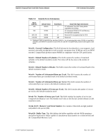
ATA Command Description SanDisk CompactFlash Card OEM Product Manual Word 21: Buffer Size. This field defines the buffer capacity of 2 sectors or 1 kilobyte of SRAM. Word 22: ECC Count. This field defines the number of ECC bytes used on each sector in the Read and Write Long commands. Words 23-26: Firmware Revision. This field contains the revision of the firmware for this product. Words 27-46: Model Number. This field contains the model number for this product and is left justified and padded with spaces (20h). Word 47: Read/Write Multiple Sector Count. This field contains the maximum number of sectors that can be read or written per interrupt using the Read Multiple or Write Multiple commands. Word 48: Double Word Support. This field indicates this product will not support double word transfers. Word 49: Capabilities. This field indicates if this product supports DMA Data transfers and LBA mode. All SanDisk products support LBA mode. Word 51: PIO Data Transfer Cycle Timing Mode. To determine the proper device timing category, compare the Cycle Time specified in Table 3-15 with the contents of this field with Table 3-14. t0 is the minimum total cycle time, t2 is the minimum command active time, and t2i is the minimum command recovery time or command inactive time. The actual cycle time equals the sum of the actual command active time and the actual command inactive time. The three timing requirements of t0, t2, and t2i shall be met. The minimum total cycle time requirements are greater than the sum of t2 and t2i. This means a host implementation may lengthen either or both t2 or t2i to ensure that t0 is equal to or greater than the value reported in the devices IDENTIFY DEVICE data. A device implementation shall support any legal host implementation. The IORD-data tri-state parameter specifies the time from the negation edge of /IORD to the time that the data bus is no longer driven by the device (tri-state). NOTE: For backward compatibility with BIOS' written before Word 64 was defined for advanced modes, a device reports in Word 51 the highest original PIO mode it can support (i.e., PIO mode 0, 1 or 2). Word 52: Single Word DMA Data Transfer Cycle Timing Mode. This field states this product does not support any Single Word DMA data transfer mode. 02/07, Rev. 12.0 5-8 © 2007 SanDisk Corporation
-
 1
1 -
2
-
3
-
4
-
5
-
6
-
7
-
8
-
9
-
10
-
11
-
12
-
13
-
14
-
15
-
16
-
17
-
18
-
19
-
20
-
21
-
22
-
23
-
24
-
25
-
26
-
27
-
28
-
29
-
30
-
31
-
32
-
33
-
34
-
35
-
36
-
37
-
38
-
39
-
40
-
41
-
42
-
43
-
44
-
45
-
46
-
47
-
48
-
49
-
50
-
51
-
52
-
53
-
54
-
55
-
56
-
 57
57 -
 58
58 -
 59
59 -
 60
60 -
 61
61 -
 62
62 -
 63
63 -
 64
64 -
 65
65 -
 66
66 -
 67
67 -
68
-
69
-
70
-
71
-
72
-
73
-
74
-
75
-
76
-
77
-
78
-
79
-
80
-
81
-
82
-
83
-
84
-
85
-
86
-
87
-
88
-
89
-
90
-
91
-
92
-
93
-
94
-
95
-
96
-
97
-
98
-
99
-
100
-
101
-
102
-
103
-
104
-
105
-
106
-
107
-
108
 |
 |