SanDisk SDCFH-004G Product Manual - Page 49
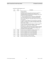
Sector Number LBA 7-0 Register Address-1F3[173]; Offset 3
 |
UPC - 878587001044
View all SanDisk SDCFH-004G manuals
Add to My Manuals
Save this manual to your list of manuals |
Page 49 highlights
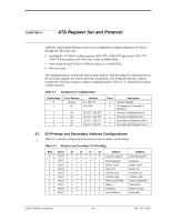
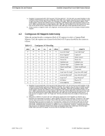
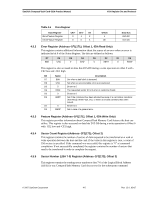
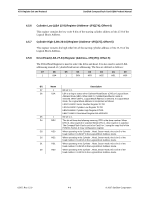
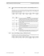
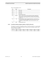
SanDisk CompactFlash Card OEM Product Manual ATA Register Set and Protocol Table 4-6 Data Register Data Register Error/Feature Register Error/Feature Register CE2- CE1- A0 0 1 X 0 0 X Offset 1 Dh Data Bus D15-D0 D15-D0 4.5.2 Error Register (Address-1F1[171]; Offset 1, 0Dh Read Only) This register contains additional information about the source of an error when an error is indicated in bit 0 of the Status Register. The bits are defined as follows: D7 D6 D5 D4 D3 D2 D1 D0 BBK UNC 0 IDNF 0 ABRT 0 AMNF This register is also accessed on data bits D15-D8 during a write operation to offset 0 with CE2 low and -CE1 high. Bit Name Description D7 BBK Set when a bad block is detected. D6 UNC Set when an uncorrectable error is encountered. D5 0 Bit set to 0. D4 IDNF The requested sector ID is in error or cannot be found. D3 0 Bit set to 0. D2 ABRT Set if the command has been aborted because of a card status condition: (Not Ready, Write Fault, etc.) or when an invalid command has been issued. D1 0 Bit set to 0. D0 AMNF Set in case of a general error. 4.5.3 Feature Register (Address-1F1[171]; Offset 1, 0Dh Write Only) This register provides information about CompactFlash Memory Card features the host can utilize. This register is also accessed on data bits D15-D8 during a write operation to Offset 0 with CE2 low and -CE1 high. 4.5.4 Sector Count Register (Address-1F2[172]; Offset 2) This register contains the number of sectors of data requested to be transferred on a read or write operation between the host and the card. If the value in this register is zero, a count of 256 sectors is specified. If the command was successful, this register is "0" at command completion. If not successfully completed, the register contains the number of sectors that need to be transferred in order to complete the request. 4.5.5 Sector Number (LBA 7-0) Register (Address-1F3[173]; Offset 3) This register contains the starting sector number or bits 7-0 of the Logical Block Address (LBA) for any CompactFlash Memory Card data access for the subsequent command. © 2007 SanDisk Corporation 4-5 Rev. 12.0, 02/07
-
 1
1 -
2
-
3
-
4
-
5
-
6
-
7
-
8
-
9
-
10
-
11
-
12
-
13
-
14
-
15
-
16
-
17
-
18
-
19
-
20
-
21
-
22
-
23
-
24
-
25
-
26
-
27
-
28
-
29
-
30
-
31
-
32
-
33
-
34
-
35
-
36
-
37
-
38
-
39
-
40
-
41
-
42
-
43
-
 44
44 -
 45
45 -
 46
46 -
 47
47 -
 48
48 -
 49
49 -
 50
50 -
 51
51 -
 52
52 -
 53
53 -
 54
54 -
55
-
56
-
57
-
58
-
59
-
60
-
61
-
62
-
63
-
64
-
65
-
66
-
67
-
68
-
69
-
70
-
71
-
72
-
73
-
74
-
75
-
76
-
77
-
78
-
79
-
80
-
81
-
82
-
83
-
84
-
85
-
86
-
87
-
88
-
89
-
90
-
91
-
92
-
93
-
94
-
95
-
96
-
97
-
98
-
99
-
100
-
101
-
102
-
103
-
104
-
105
-
106
-
107
-
108
 |
 |