SanDisk SDCFH-004G Product Manual - Page 30
Table 3-10, Common Memory Read Timing Specification, Table 3-11, Common, and Attribute Memory Write
 |
UPC - 878587001044
View all SanDisk SDCFH-004G manuals
Add to My Manuals
Save this manual to your list of manuals |
Page 30 highlights
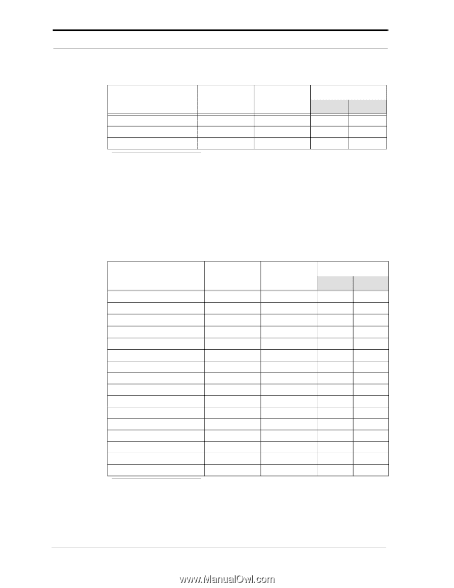
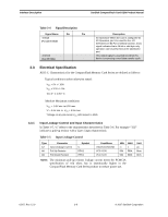
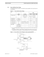
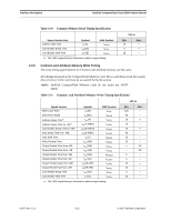
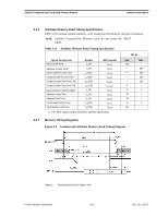
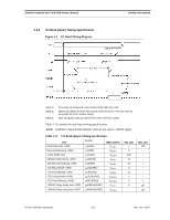
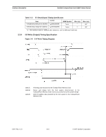
Interface Description SanDisk CompactFlash Card OEM Product Manual Table 3-10 Common Memory Read Timing Specification Speed Version Item Address Hold Time Card Enable Setup Time Card Enable Hold Time Symbol th (A) tsu(CE) th (CE) IEEE Symbol tGHAX tELGL tGHEH a. The -REG signal timing is identical to address signal timing 100 ns Min. 15 0 15 Max. ------- 3.3.5 Common and Attribute Memory Write Timing The write timing specifications for Common and Attribute memory are the same. All timings measured at the CompactFlash Memory Card. Skews and delays from the system driver/receiver to the card must be accounted for by the system NOTE: SanDisk CompactFlash Memory cards do not assert the -WAIT signal. Table 3-11 Common and Attribute Memory Write Timing Specification Speed Version Write Cycle Time Write Pulse Width Address Setup Timea Address Setup Time for -WEa Card Enable Setup Time for -WE Data Setup Time form -WE Data Hold Time Write Recover Time Output Disable Time from -WE Output Disable Time from -OE Output Enable Time from -WE Output Enable Time from -OE Output Enable Setup from -WE Output Enable Hold from -WE Card Enable Setup Time Card Enable Hold Time Symbol tc (W) tw (WE) tsu (A) tsu (A-WEH) tsu(CE-WEH) tsu(D-WEH) th (D) trec (WE) tdis (WE) tdis (OE) ten (WE) ten (OE) tsu(OE-WE) th(OE-WE) tsu (CE) th (CE) IEEE Symbol tAVAV tWLWH tAVWL tAVWH tELWH tDVWH tWMDX tWMAX tWLQZ tGHQZ tWHQNZ tGLQNZ tGHWL tWHGL tELWL tGHEH a. The -REG signal timing is identical to address signal timing. 100 ns Min. 100 60 10 70 70 40 15 15 ----- 5 5 10 10 0 15 Max 50 50 02/07, Rev. 12.0 3-12 © 2007 SanDisk Corporation
-
 1
1 -
2
-
3
-
4
-
5
-
6
-
7
-
8
-
9
-
10
-
11
-
12
-
13
-
14
-
15
-
16
-
17
-
18
-
19
-
20
-
21
-
22
-
23
-
24
-
 25
25 -
 26
26 -
 27
27 -
 28
28 -
 29
29 -
 30
30 -
 31
31 -
 32
32 -
 33
33 -
 34
34 -
 35
35 -
36
-
37
-
38
-
39
-
40
-
41
-
42
-
43
-
44
-
45
-
46
-
47
-
48
-
49
-
50
-
51
-
52
-
53
-
54
-
55
-
56
-
57
-
58
-
59
-
60
-
61
-
62
-
63
-
64
-
65
-
66
-
67
-
68
-
69
-
70
-
71
-
72
-
73
-
74
-
75
-
76
-
77
-
78
-
79
-
80
-
81
-
82
-
83
-
84
-
85
-
86
-
87
-
88
-
89
-
90
-
91
-
92
-
93
-
94
-
95
-
96
-
97
-
98
-
99
-
100
-
101
-
102
-
103
-
104
-
105
-
106
-
107
-
108
 |
 |