SanDisk SDCFH-004G Product Manual - Page 39
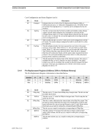
Table 3-17, Registers and Memory Space Decoding
 |
UPC - 878587001044
View all SanDisk SDCFH-004G manuals
Add to My Manuals
Save this manual to your list of manuals |
Page 39 highlights
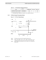
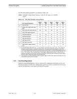
SanDisk CompactFlash Card OEM Product Manual Interface Description In addition, these registers provide a method for accessing status information about the card that may be used to arbitrate between multiple interrupt sources on the same interrupt level or to replace status information that appears on dedicated pins in memory cards that have alternate use in I/O cards. Table 3-17 Registers and Memory Space Decoding A8-CE2 -CE1 -REG -OE -WE A10 A9 A4 A3 A2 A1 A0 Selected Space 1 1 X X X X X XX X X X X Standby X 0 0 0 1 X 1 XX X X X 0 Configuration Registers Read 1 0 1 0 1 X X XX X X X X Common Memory Read (8-bit D7-D0) 0 1 1 0 1 X X XX X X X X Common Memory Read (8-bit D15-D8) 0 0 1 0 1 X X XX X X X 0 Common Memory Read (16-bit D15-D0) X 0 0 1 0 X 1 XX X X X 0 Configuration Registers Write 1 0 1 1 0 X X XX X X X X Common Memory Write (8- bit D7-D0) 0 1 1 1 0 X X XX X X X X Common Memory Write (8- bit D15-D8) 0 0 1 1 0 X X XX X X X 0 Common Memory Write (16-bit D15-D0) X 0 0 0 1 0 0 XX X X X 0 Card Info Structure Read 1 0 0 1 0 0 0 XX X X X 0 Invalid Access (CIS Write) 1 0 0 0 1 X X XX X X X 1 Invalid Access (Odd Attribute Read) 1 0 0 1 0 X X XX X X X 1 Invalid Access (Odd Attribute Write) 0 1 0 0 1 X X XX X X X X Invalid Access (Odd Attribute Read) 0 1 0 1 0 X X XX X X X X Invalid Access (Odd Attribute Write) NOTE: The location of the card configuration registers should always be read from the CIS since these locations may vary in future products. No writes should be performed to the card attribute memory except to the card configuration register addresses. All other attribute memory locations are reserved. © 2007 SanDisk Corporation 3-21 Rev. 12.0, 02/07
-
 1
1 -
2
-
3
-
4
-
5
-
6
-
7
-
8
-
9
-
10
-
11
-
12
-
13
-
14
-
15
-
16
-
17
-
18
-
19
-
20
-
21
-
22
-
23
-
24
-
25
-
26
-
27
-
28
-
29
-
30
-
31
-
32
-
33
-
 34
34 -
 35
35 -
 36
36 -
 37
37 -
 38
38 -
 39
39 -
 40
40 -
 41
41 -
 42
42 -
 43
43 -
 44
44 -
45
-
46
-
47
-
48
-
49
-
50
-
51
-
52
-
53
-
54
-
55
-
56
-
57
-
58
-
59
-
60
-
61
-
62
-
63
-
64
-
65
-
66
-
67
-
68
-
69
-
70
-
71
-
72
-
73
-
74
-
75
-
76
-
77
-
78
-
79
-
80
-
81
-
82
-
83
-
84
-
85
-
86
-
87
-
88
-
89
-
90
-
91
-
92
-
93
-
94
-
95
-
96
-
97
-
98
-
99
-
100
-
101
-
102
-
103
-
104
-
105
-
106
-
107
-
108
 |
 |