SanDisk SDCFH-004G Product Manual - Page 52
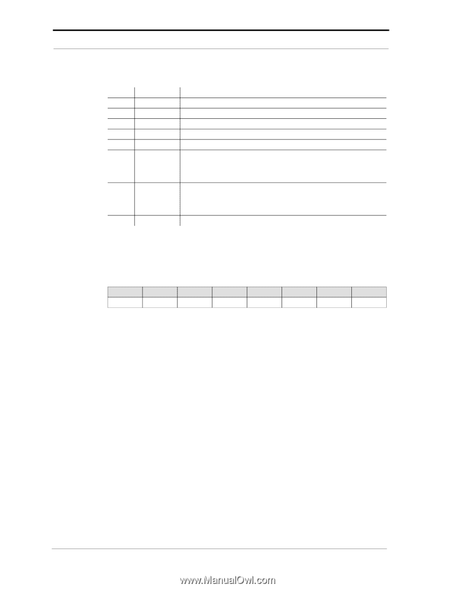
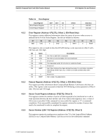
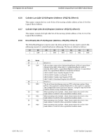
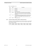
Card Drive Address Register Address-3F7[377]; Offset Fh
 |
UPC - 878587001044
View all SanDisk SDCFH-004G manuals
Add to My Manuals
Save this manual to your list of manuals |
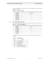
Page 52 highlights
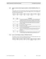
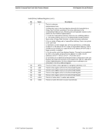
ATA Register Set and Protocol SanDisk CompactFlash Card OEM Product Manual Device Control Register (con't) Bit Name Description D7 X Don't care. D6 X Don't care. D5 X Don't care. D4 X Don't care. D3 1 Bit ignored by the card. D2 SW Rst Set to 1 in order to force the card to perform an AT Disk controller Soft Reset operation. This does not change the PCMCIA Card Configuration registers as a hardware reset does. The card remains in Reset until this bit is reset to "0". D1 -IEn Interrupt Enable bit enables interrupts when the bit is 0. When the bit is 1, interrupts from the card are disabled. This bit also controls the Int bit in the Configuration and Status Register. This bit is set to 0 at power on and reset. D0 ERR Bit ignored by the card. 4.5.11 Card (Drive) Address Register (Address-3F7[377]; Offset Fh) This register is provided for compatibility with the AT disk drive interface. It is recommended that this register not be mapped into the host's I/O space because of potential conflicts on Bit 7. The bits are defined as follows: D7 D6 D5 D4 D3 D2 D1 D0 X -WTG -HS3 -HS2 -HS1 -HS0 -nDS1 -nDS0 02/07, Rev. 12.0 4-8 © 2007 SanDisk Corporation
-
 1
1 -
2
-
3
-
4
-
5
-
6
-
7
-
8
-
9
-
10
-
11
-
12
-
13
-
14
-
15
-
16
-
17
-
18
-
19
-
20
-
21
-
22
-
23
-
24
-
25
-
26
-
27
-
28
-
29
-
30
-
31
-
32
-
33
-
34
-
35
-
36
-
37
-
38
-
39
-
40
-
41
-
42
-
43
-
44
-
45
-
46
-
 47
47 -
 48
48 -
 49
49 -
 50
50 -
 51
51 -
 52
52 -
 53
53 -
 54
54 -
 55
55 -
 56
56 -
 57
57 -
58
-
59
-
60
-
61
-
62
-
63
-
64
-
65
-
66
-
67
-
68
-
69
-
70
-
71
-
72
-
73
-
74
-
75
-
76
-
77
-
78
-
79
-
80
-
81
-
82
-
83
-
84
-
85
-
86
-
87
-
88
-
89
-
90
-
91
-
92
-
93
-
94
-
95
-
96
-
97
-
98
-
99
-
100
-
101
-
102
-
103
-
104
-
105
-
106
-
107
-
108
 |
 |