Fujitsu MPD3173AT Product Manual - Page 74
Table 5.3, I/O registers, Notes
 |
View all Fujitsu MPD3173AT manuals
Add to My Manuals
Save this manual to your list of manuals |
Page 74 highlights
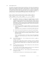
Table 5.3 I/O registers CS0- CS1- DA2 DA1 I/O registers DA0 Read operation Write operation Command block registers 1 0 0 0 0 Data Data 1 0 0 0 1 Error Register Features 1 0 0 1 0 Sector Count Sector Count 1 0 0 1 1 Sector Number Sector Number 1 0 1 0 0 Cylinder Low Cylinder Low 1 0 1 0 1 Cylinder High Cylinder High 1 0 1 1 0 Device/Head Device/Head 1 0 1 1 1 Status Command 1 1 X X X (Invalid) (Invalid) Control block registers 0 1 1 1 0 Alternate Status Device Control 0 1 1 1 1 - - Host I/O address X'1F0' X'1F1' X'1F2' X'1F3' X'1F4' X'1F5' X'1F6' X'1F7' - X'3F6' X'3F7' Notes: 1. The Data register for read or write operation can be accessed by 16 bit data bus (DATA0 to DATA15). 2. The registers for read or write operation other than the Data registers can be accessed by 8 bit data bus (DATA0 to DATA7). 3. When reading the Drive Address register, bit 7 is high-impedance state. 4. The LBA mode is specified, the Device/Head, Cylinder High, Cylinder Low, and Sector Number registers indicate LBA bits 27 to 24, 23 to 16, 15 to 8, and 7 to 0. C141-E069-02EN 5 - 7
-
 1
1 -
2
-
3
-
4
-
5
-
6
-
7
-
8
-
9
-
10
-
11
-
12
-
13
-
14
-
15
-
16
-
17
-
18
-
19
-
20
-
21
-
22
-
23
-
24
-
25
-
26
-
27
-
28
-
29
-
30
-
31
-
32
-
33
-
34
-
35
-
36
-
37
-
38
-
39
-
40
-
41
-
42
-
43
-
44
-
45
-
46
-
47
-
48
-
49
-
50
-
51
-
52
-
53
-
54
-
55
-
56
-
57
-
58
-
59
-
60
-
61
-
62
-
63
-
64
-
65
-
66
-
67
-
68
-
 69
69 -
 70
70 -
 71
71 -
 72
72 -
 73
73 -
 74
74 -
 75
75 -
 76
76 -
 77
77 -
 78
78 -
 79
79 -
80
-
81
-
82
-
83
-
84
-
85
-
86
-
87
-
88
-
89
-
90
-
91
-
92
-
93
-
94
-
95
-
96
-
97
-
98
-
99
-
100
-
101
-
102
-
103
-
104
-
105
-
106
-
107
-
108
-
109
-
110
-
111
-
112
-
113
-
114
-
115
-
116
-
117
-
118
-
119
-
120
-
121
-
122
-
123
-
124
-
125
-
126
-
127
-
128
-
129
-
130
-
131
-
132
-
133
-
134
-
135
-
136
-
137
-
138
-
139
-
140
-
141
-
142
-
143
-
144
-
145
-
146
-
147
-
148
-
149
-
150
-
151
-
152
-
153
-
154
-
155
-
156
-
157
-
158
-
159
-
160
-
161
-
162
-
163
-
164
-
165
-
166
-
167
-
168
-
169
-
170
-
171
-
172
-
173
-
174
-
175
-
176
-
177
-
178
-
179
-
180
-
181
-
182
-
183
-
184
-
185
-
186
-
187
-
188
-
189
-
190
-
191
 |
 |
