Nintendo DMG-01 Manual - Page 137
Typical timing diagram
 |
View all Nintendo DMG-01 manuals
Add to My Manuals
Save this manual to your list of manuals |
Page 137 highlights
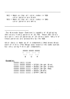
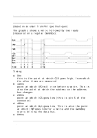
Game BoyTM CPU Manual 5.2. Typical timing diagram 5.2. Typical timing diagram (Based on an email from Philippe Pouliquen) The graphic shows a write followed by two reads (measured on a regular GameBoy): _________ _________ _________ ___ CLK:____/ \_________/ \_________/ \_________/ /RD:_______/ /WR: \_______/ __________ _____ _____ ___ /CS: Adr Bus:_______X X X X_ Dta: _________ _________ _________ Bus ^^^ ^ ^ ^^ Time: a b c d e fg Timing: a: 0ns this is the point at which CLK goes high, from which the other times are measured. b: 140ns point at which /RD will rise before a write. This is also the point at which the address on the address bus changes. c: 240ns point at which /CS goes low (this is pin 5 of the connector) d: 480ns point at which CLK goes low. This is also the point at which /WR goes low for a write and the GameBoy starts driving the data bus. e: 840ns by DP Page 137
-
 1
1 -
2
-
3
-
4
-
5
-
6
-
7
-
8
-
9
-
10
-
11
-
12
-
13
-
14
-
15
-
16
-
17
-
18
-
19
-
20
-
21
-
22
-
23
-
24
-
25
-
26
-
27
-
28
-
29
-
30
-
31
-
32
-
33
-
34
-
35
-
36
-
37
-
38
-
39
-
40
-
41
-
42
-
43
-
44
-
45
-
46
-
47
-
48
-
49
-
50
-
51
-
52
-
53
-
54
-
55
-
56
-
57
-
58
-
59
-
60
-
61
-
62
-
63
-
64
-
65
-
66
-
67
-
68
-
69
-
70
-
71
-
72
-
73
-
74
-
75
-
76
-
77
-
78
-
79
-
80
-
81
-
82
-
83
-
84
-
85
-
86
-
87
-
88
-
89
-
90
-
91
-
92
-
93
-
94
-
95
-
96
-
97
-
98
-
99
-
100
-
101
-
102
-
103
-
104
-
105
-
106
-
107
-
108
-
109
-
110
-
111
-
112
-
113
-
114
-
115
-
116
-
117
-
118
-
119
-
120
-
121
-
122
-
123
-
124
-
125
-
126
-
127
-
128
-
129
-
130
-
131
-
 132
132 -
 133
133 -
 134
134 -
 135
135 -
 136
136 -
 137
137 -
 138
138 -
 139
139
 |
 |
