Nintendo DMG-01 Manual - Page 39
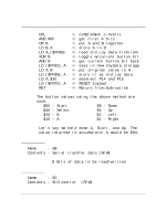
FF06 TMA, FF07 TAC, FF0F IF
 |
View all Nintendo DMG-01 manuals
Add to My Manuals
Save this manual to your list of manuals |
Page 39 highlights
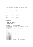
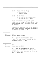
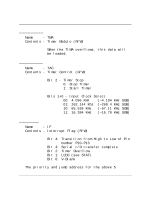
Game BoyTM CPU Manual 2.13.1. I/O Registers 6. FF06 (TMA) Name - TMA Contents - Timer Modulo (R/W) When the TIMA overflows, this data will be loaded. 7. FF07 (TAC) Name - TAC Contents - Timer Control (R/W) Bit 2 - Timer Stop 0: Stop Timer 1: Start Timer Bits 1+0 - Input Clock Select 00: 4.096 KHz (~4.194 KHz SGB) 01: 262.144 Khz (~268.4 KHz SGB) 10: 65.536 KHz (~67.11 KHz SGB) 11: 16.384 KHz (~16.78 KHz SGB) 8. FF0F (IF) Name - IF Contents - Interrupt Flag (R/W) Bit 4: Transition from High to Low of Pin number P10-P13 Bit 3: Serial I/O transfer complete Bit 2: Timer Overflow Bit 1: LCDC (see STAT) Bit 0: V-Blank The priority and jump address for the above 5 by DP Page 39
-
 1
1 -
2
-
3
-
4
-
5
-
6
-
7
-
8
-
9
-
10
-
11
-
12
-
13
-
14
-
15
-
16
-
17
-
18
-
19
-
20
-
21
-
22
-
23
-
24
-
25
-
26
-
27
-
28
-
29
-
30
-
31
-
32
-
33
-
 34
34 -
 35
35 -
 36
36 -
 37
37 -
 38
38 -
 39
39 -
 40
40 -
 41
41 -
 42
42 -
 43
43 -
 44
44 -
45
-
46
-
47
-
48
-
49
-
50
-
51
-
52
-
53
-
54
-
55
-
56
-
57
-
58
-
59
-
60
-
61
-
62
-
63
-
64
-
65
-
66
-
67
-
68
-
69
-
70
-
71
-
72
-
73
-
74
-
75
-
76
-
77
-
78
-
79
-
80
-
81
-
82
-
83
-
84
-
85
-
86
-
87
-
88
-
89
-
90
-
91
-
92
-
93
-
94
-
95
-
96
-
97
-
98
-
99
-
100
-
101
-
102
-
103
-
104
-
105
-
106
-
107
-
108
-
109
-
110
-
111
-
112
-
113
-
114
-
115
-
116
-
117
-
118
-
119
-
120
-
121
-
122
-
123
-
124
-
125
-
126
-
127
-
128
-
129
-
130
-
131
-
132
-
133
-
134
-
135
-
136
-
137
-
138
-
139
 |
 |

Game Boy
TM
CPU Manual
2.13.1. I/O Registers
6.
FF06 (TMA)
Name
- TMA
Contents - Timer Modulo (R/W)
When the TIMA overflows, this data will
be loaded.
7.
FF07 (TAC)
Name
- TAC
Contents - Timer Control (R/W)
Bit 2 - Timer Stop
0: Stop Timer
1: Start Timer
Bits 1+0 - Input Clock Select
00: 4.096 KHz
(~4.194 KHz SGB)
01: 262.144 Khz
(~268.4 KHz SGB)
10: 65.536 KHz
(~67.11 KHz SGB)
11: 16.384 KHz
(~16.78 KHz SGB)
8.
FF0F (IF)
Name
- IF
Contents - Interrupt Flag (R/W)
Bit 4: Transition from High to Low of Pin
number P10-P13
Bit 3: Serial I/O transfer complete
Bit 2: Timer Overflow
Bit 1: LCDC (see STAT)
Bit 0: V-Blank
The priority and jump address for the above 5
by DP
Page 39