Nintendo DMG-01 Manual - Page 138
V 1.01
 |
View all Nintendo DMG-01 manuals
Add to My Manuals
Save this manual to your list of manuals |
Page 138 highlights
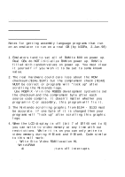
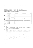
5.2. Typical timing diagram Game BoyTM CPU Manual point at which /WR goes high after a write. f: 960ns point at which CLK goes high. This is also the point at which /CS goes high and the GameBoy stops driving the data bus. g: 990ns point at which /RD goes low for a read (30ns after CLK goes high). (Measurements roundet to the nearest 10ns) "Some devices (like disk controller chips) require that the address be valid before you access them (with a read or write pulse). The problem is that /RD doesn't go high between consecutive reads, and the second problem is that when /RD transitions, it does so at the same time (or before) the address changes. The result is that from the device's perspective, an address transition looks like a bunch of reads from random addresses. These spurious reads are ok for RAM and ROM, but can really screw things up for devices with internal buffers, because they may be fooled into thinking that you have read more data from them than you actually have. The way to solve this problem is to feed CLK and /RD through a OR gate. The downside is that it makes your allowable read time shorter. Page 138 V 1.01
-
 1
1 -
2
-
3
-
4
-
5
-
6
-
7
-
8
-
9
-
10
-
11
-
12
-
13
-
14
-
15
-
16
-
17
-
18
-
19
-
20
-
21
-
22
-
23
-
24
-
25
-
26
-
27
-
28
-
29
-
30
-
31
-
32
-
33
-
34
-
35
-
36
-
37
-
38
-
39
-
40
-
41
-
42
-
43
-
44
-
45
-
46
-
47
-
48
-
49
-
50
-
51
-
52
-
53
-
54
-
55
-
56
-
57
-
58
-
59
-
60
-
61
-
62
-
63
-
64
-
65
-
66
-
67
-
68
-
69
-
70
-
71
-
72
-
73
-
74
-
75
-
76
-
77
-
78
-
79
-
80
-
81
-
82
-
83
-
84
-
85
-
86
-
87
-
88
-
89
-
90
-
91
-
92
-
93
-
94
-
95
-
96
-
97
-
98
-
99
-
100
-
101
-
102
-
103
-
104
-
105
-
106
-
107
-
108
-
109
-
110
-
111
-
112
-
113
-
114
-
115
-
116
-
117
-
118
-
119
-
120
-
121
-
122
-
123
-
124
-
125
-
126
-
127
-
128
-
129
-
130
-
131
-
132
-
 133
133 -
 134
134 -
 135
135 -
 136
136 -
 137
137 -
 138
138 -
 139
139
 |
 |
