Nintendo DMG-01 Manual - Page 9
Echo of 8kB Internal RAM, User I/O
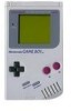 |
View all Nintendo DMG-01 manuals
Add to My Manuals
Save this manual to your list of manuals |
Page 9 highlights
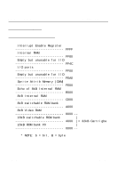
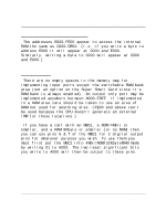
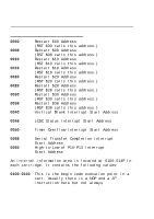
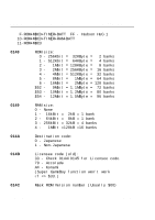
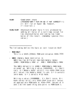
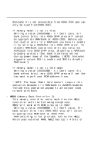
Game BoyTM CPU Manual 2.5.2. Echo of 8kB Internal RAM 2.5.2. Echo of 8kB Internal RAM The addresses E000-FE00 appear to access the internal RAM the same as C000-DE00. (i.e. If you write a byte to address E000 it will appear at C000 and E000. Similarly, writing a byte to C000 will appear at C000 and E000.) 2.5.3. User I/O There are no empty spaces in the memory map for implementing input ports except the switchable RAM bank area (not an option on the Super Smart Card since it's RAM bank is always enabled). An output only port may be implemented anywhere between A000-FDFF. If implemented in a RAM area care should be taken to use an area of RAM not used for anything else. (FE00 and above can't be used because the CPU doesn't generate an external /WR for these locations.) If you have a cart with an MBC1, a ROM 4Mbit or smaller, and a RAM 8Kbyte or smaller (or no RAM) then you can use pins 6 & 7 of the MBC1 for 2 digital output pins for whatever purpose you wish. To use them you must first put the MBC1 into 4MbitROM/32KbyteRAM mode by writing 01 to 6000. The two least significant bits you write to 4000 will then be output to these pins. by DP Page 9
-
 1
1 -
2
-
3
-
 4
4 -
 5
5 -
 6
6 -
 7
7 -
 8
8 -
 9
9 -
 10
10 -
 11
11 -
 12
12 -
 13
13 -
 14
14 -
15
-
16
-
17
-
18
-
19
-
20
-
21
-
22
-
23
-
24
-
25
-
26
-
27
-
28
-
29
-
30
-
31
-
32
-
33
-
34
-
35
-
36
-
37
-
38
-
39
-
40
-
41
-
42
-
43
-
44
-
45
-
46
-
47
-
48
-
49
-
50
-
51
-
52
-
53
-
54
-
55
-
56
-
57
-
58
-
59
-
60
-
61
-
62
-
63
-
64
-
65
-
66
-
67
-
68
-
69
-
70
-
71
-
72
-
73
-
74
-
75
-
76
-
77
-
78
-
79
-
80
-
81
-
82
-
83
-
84
-
85
-
86
-
87
-
88
-
89
-
90
-
91
-
92
-
93
-
94
-
95
-
96
-
97
-
98
-
99
-
100
-
101
-
102
-
103
-
104
-
105
-
106
-
107
-
108
-
109
-
110
-
111
-
112
-
113
-
114
-
115
-
116
-
117
-
118
-
119
-
120
-
121
-
122
-
123
-
124
-
125
-
126
-
127
-
128
-
129
-
130
-
131
-
132
-
133
-
134
-
135
-
136
-
137
-
138
-
139
 |
 |
