SanDisk SDSDH-1024 Product Manual - Page 109
Table 5-5, Timing Constants Definitions
 |
UPC - 710348911073
View all SanDisk SDSDH-1024 manuals
Add to My Manuals
Save this manual to your list of manuals |
Page 109 highlights
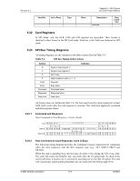
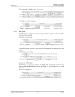
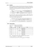
Revision 2.2 Chapter 5 - SPI Protocol SD Card Product Manual 5.23.4 Data Write The host may de-select a card (by raising the CS) at any time during the card busy period. The card will release the DataOut line one clock after the CS going high. To check if the card is still busy it needs to be re-selected by asserting (set to low) the CS signal. The card will resume busy signal (pulling DataOut low) one clock after the falling edge of CS. Device Write Timing CS Data In Data Out HL L L L L L L L L HHHL L L L NCS XHHH write command HHHH NWR HHH data block NEC NDS H H H HH H XX X H H HH Z Z H H H ******** NCR H H H card resp. H H H H H H H data response busy L Z Z Z busy H The following figure describes stop transmission operation in Multiple Block Write transfer. The "busy" may appear within NBR clocks after Stop Tran token. If there is no busy, the host may continue to the next command. Stop Transmission Timing-Multiple Block Write CS Data In L L L LL L L L L L L L L L L L L L L L L L HHH L L L L data block NW R HH H H H H H H H 1byte stop tran token NBR NEC HHH NDS XXXHHHH Data Out H H H H data resp. busy H H H H H H H H H busy L Z Z Z busy H 5.24 Timing Values Table 5-5 shows the timing values and definitions. Table 5-5 Timing Constants Definitions Value Min. Max. Unit NCS 0 --- 8 Clock cycles NCR 1 8 8 Clock cycles NRC 1 --- 8 Clock cycles NAC 1 See Note 8 Clock cycles NWR 1 --- 8 Clock cycles NEC 0 --- 8 Clock cycles NDS 0 --- 8 Clock cycles NBR 0 1 8 Clock cycles NCX 0 8 8 Clock cycles Note: The maximum read access time is calculated by the host as follows. NAC(max)= 100 ((TAAC * fPP) + (100 * NSAC)) ; fPP is the interface clock rate and TAAC & NSAC are given in the CSD Register. © 2004 SanDisk Corporation 5-19 12/08/04
-
 1
1 -
2
-
3
-
4
-
5
-
6
-
7
-
8
-
9
-
10
-
11
-
12
-
13
-
14
-
15
-
16
-
17
-
18
-
19
-
20
-
21
-
22
-
23
-
24
-
25
-
26
-
27
-
28
-
29
-
30
-
31
-
32
-
33
-
34
-
35
-
36
-
37
-
38
-
39
-
40
-
41
-
42
-
43
-
44
-
45
-
46
-
47
-
48
-
49
-
50
-
51
-
52
-
53
-
54
-
55
-
56
-
57
-
58
-
59
-
60
-
61
-
62
-
63
-
64
-
65
-
66
-
67
-
68
-
69
-
70
-
71
-
72
-
73
-
74
-
75
-
76
-
77
-
78
-
79
-
80
-
81
-
82
-
83
-
84
-
85
-
86
-
87
-
88
-
89
-
90
-
91
-
92
-
93
-
94
-
95
-
96
-
97
-
98
-
99
-
100
-
101
-
102
-
103
-
 104
104 -
 105
105 -
 106
106 -
 107
107 -
 108
108 -
 109
109 -
 110
110 -
 111
111 -
 112
112 -
 113
113 -
 114
114 -
115
-
116
-
117
-
118
-
119
-
120
-
121
-
122
-
123
 |
 |
