SanDisk SDSDH-1024 Product Manual - Page 90
Timing Values
 |
UPC - 710348911073
View all SanDisk SDSDH-1024 manuals
Add to My Manuals
Save this manual to your list of manuals |
Page 90 highlights
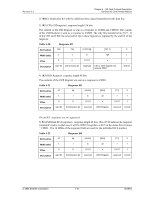
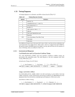
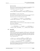
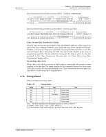
Revision 2.2 Chapter 4 - SD Card Protocol Description SanDisk SD Card Product Manual Stop Transmission Received after Last Data Block-Card Busy Programming Host Command NCRCycles Card Response Host Command CMD S T Content CRC E Z Z P *** P S T Content CRC E S T Content Card is Programming DAT S L L EZ Z Z Z Z Z Z Z Stop Transmission Received after Last Data Block-Card becomes Busy Host Command NCRCycles CMD S T Content CRC E Z Z P *** DAT Z Z Z Z Z Z Z Z Z Z Z S L Card Response P S T Content CRC Card is Programming Host Command E ST Content L EZ Z Z Z Z Z Z Z Erase, Set and Clear Write Protect Timing The host must first tag the start (CMD32) and end (CMD33) addresses of the range to be erased. The erase command (CMD38), once issued, will erase all the selected write blocks. Similarly, set and clear write protect commands start a programming operation as well. The card will signal "busy" (by pulling the DAT line low) for the duration of the erase or programming operation. The bus transaction timings are the same as given for stop tran command in the "Stop Transmission Received after Last Data Block-Card Busy Programming" diagram above. Re-selecting a Busy Card When a busy card, which is currently in the dis state, is reselected it will reinstate its busy signaling on the data line. The timing diagram for this command/response/busy transaction is the same as given for stop tran command in the "Stop Transmission Received after Last Data Block-Card becomes Busy" diagram above. 4.13 Timing Values Table 4-24 defines all timing values. Table 4-24 Timing Values Value Min. Max. Unit NCR 2 64 Clock cycles NID 5 5 Clock cycles NAC 2 See Note Clock cycles NRC 8 --- Clock cycles NCC 8 --- Clock cycles NWR 2 --- Clock cycles Note-The host calculates the maximum read access time as follows: NAC(max)= 100 ((TAAC * fPP) + (100 * NSAC)) ; fPP is the interface clock rate and TAAC & NSAC are given in the CSD Register. © 2004 SanDisk Corporation 4-46 12/08/04
-
 1
1 -
2
-
3
-
4
-
5
-
6
-
7
-
8
-
9
-
10
-
11
-
12
-
13
-
14
-
15
-
16
-
17
-
18
-
19
-
20
-
21
-
22
-
23
-
24
-
25
-
26
-
27
-
28
-
29
-
30
-
31
-
32
-
33
-
34
-
35
-
36
-
37
-
38
-
39
-
40
-
41
-
42
-
43
-
44
-
45
-
46
-
47
-
48
-
49
-
50
-
51
-
52
-
53
-
54
-
55
-
56
-
57
-
58
-
59
-
60
-
61
-
62
-
63
-
64
-
65
-
66
-
67
-
68
-
69
-
70
-
71
-
72
-
73
-
74
-
75
-
76
-
77
-
78
-
79
-
80
-
81
-
82
-
83
-
84
-
 85
85 -
 86
86 -
 87
87 -
 88
88 -
 89
89 -
 90
90 -
 91
91 -
 92
92 -
 93
93 -
 94
94 -
 95
95 -
96
-
97
-
98
-
99
-
100
-
101
-
102
-
103
-
104
-
105
-
106
-
107
-
108
-
109
-
110
-
111
-
112
-
113
-
114
-
115
-
116
-
117
-
118
-
119
-
120
-
121
-
122
-
123
 |
 |
