SanDisk SDSDH-1024 Product Manual - Page 28
Table 3-5, Host and Bus Capacities, Bus Signal Levels, Table 3-6, Input/Output Voltage - 90
 |
UPC - 710348911073
View all SanDisk SDSDH-1024 manuals
Add to My Manuals
Save this manual to your list of manuals |
Page 28 highlights
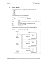
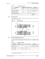
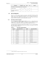
Revision 2.2 Chapter 3 - SD Card Interface Description SD Card Product Manual Table 3-5 Host and Bus Capacities8 Parameter Pull-up resistance Bus signal line capacitance Bus signal line capacitance Signal card capacitance Max. signal line inductance Pull-up resistance inside card (pin 1) Symbol RCMD, RDAT CL CL CCARD --RDAT3 Min. 10 --------10 Max. 100 250 100 10 16 90 Unit Remark kΩ Prevents bus floating pF fPP < 5 MHz, 21 cards pF fPP < 20 MHz, 7 cards pF nH fPP
-
 1
1 -
2
-
3
-
4
-
5
-
6
-
7
-
8
-
9
-
10
-
11
-
12
-
13
-
14
-
15
-
16
-
17
-
18
-
19
-
20
-
21
-
22
-
 23
23 -
 24
24 -
 25
25 -
 26
26 -
 27
27 -
 28
28 -
 29
29 -
 30
30 -
 31
31 -
 32
32 -
 33
33 -
34
-
35
-
36
-
37
-
38
-
39
-
40
-
41
-
42
-
43
-
44
-
45
-
46
-
47
-
48
-
49
-
50
-
51
-
52
-
53
-
54
-
55
-
56
-
57
-
58
-
59
-
60
-
61
-
62
-
63
-
64
-
65
-
66
-
67
-
68
-
69
-
70
-
71
-
72
-
73
-
74
-
75
-
76
-
77
-
78
-
79
-
80
-
81
-
82
-
83
-
84
-
85
-
86
-
87
-
88
-
89
-
90
-
91
-
92
-
93
-
94
-
95
-
96
-
97
-
98
-
99
-
100
-
101
-
102
-
103
-
104
-
105
-
106
-
107
-
108
-
109
-
110
-
111
-
112
-
113
-
114
-
115
-
116
-
117
-
118
-
119
-
120
-
121
-
122
-
123
 |
 |

Chapter 3 – SD Card Interface Description
Revision 2.2
SD Card Product Manual
© 2004 SanDisk Corporation
3-8
12/08/04
Table 3-5
Host and Bus Capacities
8
Parameter
Symbol
Min.
Max.
Unit
Remark
Pull-up resistance
R
CMD,
R
DAT
10
100
k
Ω
Prevents bus floating
Bus signal line capacitance
C
L
---
250
pF
f
PP
<
5 MHz, 21 cards
Bus signal line capacitance
C
L
---
100
pF
Signal card capacitance
C
CARD
---
10
pF
f
PP
<
20 MHz, 7 cards
Max. signal line inductance
---
---
16
nH
f
PP
<
20 MHz
Pull-up resistance inside card (pin 1)
R
DAT3
10
90
k
Ω
May be used for card
detection
3.4.4
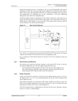
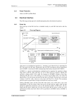
Bus Signal Levels
All signal levels are related to the supply voltage because the bus can have a variable
supply voltage (see Figure 3-6).
Figure 3-6
Bus Signal Levels
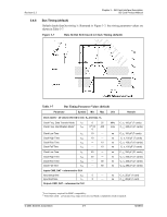
3.4.5
Open-drain Mode Bus Signal Level
To meet the requirements of the JEDEC specification JESD8-1A, the card input and output
voltages are within the specified ranges in Table 3-6 for any V
DD
of the allowed voltage
range.
Table 3-6
Input/Output Voltage
Parameter
Symbol
Min.
Max.
Unit
Conditions
Output high voltage
V
OH
0.75*V
DD
---
V
I
OH
= -100 uA@ V
DD
(minimum)
Output low voltage
V
OL
---
0.125*V
DD
V
I
OL
= 100 uA@ V
DD
(minimum)
Input high voltage
V
IH
0.625*V
DD
V
DD
+0.3
V
---
Input low voltage
V
IL
V
SS
-0.3
0.25*V
DD
V
---
8
The total capacitance of CMD and DAT lines will consist of C
HOST
, C
BUS
, and one C
CARD
only because they are
connected separately to the SD Card host.
Input
Low
Level
Input
High
Level
Output
High
Level
Output
Low
Level
Undefined
V
DD
V
OH
V
IH
V
L
V
OL
V
SS
t
V