SanDisk SDSDH-1024 Product Manual - Page 30
Data In/Out Referenced to Clock Timing high-speed, Table 3-8, Bus Timing Parameter
 |
UPC - 710348911073
View all SanDisk SDSDH-1024 manuals
Add to My Manuals
Save this manual to your list of manuals |
Page 30 highlights
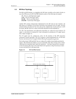
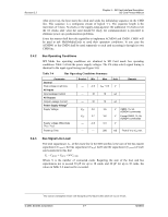
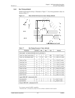
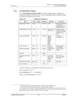
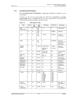
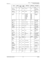
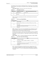
Revision 2.2 Chapter 3 - SD Card Interface Description SD Card Product Manual Parameter Symbol Min Max Clock (CLK) - all values referred to min. VIH and max. VIL Output delay time during Data tOSU 0 14 Transfer mode Output delay time during Identification mode tODLY 0 50 Unit Remark ns CL < 25 pF (1 card) ns CL < 25 pF (1 card) 3.4.7 Bus Timing (high-speed mode) High-speed mode dataIn/dataOut timing is illustrated in Figure 3-8; bus timing parameter values are shown in Table 3-8. Figure 3-8 Data In/Out Referenced to Clock Timing (high-speed) Table 3-8 Bus Timing Parameter Values (high-speed) Parameter Symbol Min Max Unit Clock (CLK) - all values referred to min. VIH and max. VIL Clock Freq. Data Transfer Mode fPP Clock Low Time tWL 0 50 7 --- Clock High Time tWH 7 --- Clock Rise Time tTLH --- 3 Clock Fall Time tTHL --- 3 MHz ns ns ns ns Inputs CMD, DAT - referenced to CLK Input setup time Input hold time tISU 6 --- ns tIH 2 --- ns Outputs CMD, DAT - referenced to CLK Output delay time during Data tODLY --- 14 ns Transfer mode Remark © 2004 SanDisk Corporation 3-10 12/08/04
-
 1
1 -
2
-
3
-
4
-
5
-
6
-
7
-
8
-
9
-
10
-
11
-
12
-
13
-
14
-
15
-
16
-
17
-
18
-
19
-
20
-
21
-
22
-
23
-
24
-
 25
25 -
 26
26 -
 27
27 -
 28
28 -
 29
29 -
 30
30 -
 31
31 -
 32
32 -
 33
33 -
 34
34 -
 35
35 -
36
-
37
-
38
-
39
-
40
-
41
-
42
-
43
-
44
-
45
-
46
-
47
-
48
-
49
-
50
-
51
-
52
-
53
-
54
-
55
-
56
-
57
-
58
-
59
-
60
-
61
-
62
-
63
-
64
-
65
-
66
-
67
-
68
-
69
-
70
-
71
-
72
-
73
-
74
-
75
-
76
-
77
-
78
-
79
-
80
-
81
-
82
-
83
-
84
-
85
-
86
-
87
-
88
-
89
-
90
-
91
-
92
-
93
-
94
-
95
-
96
-
97
-
98
-
99
-
100
-
101
-
102
-
103
-
104
-
105
-
106
-
107
-
108
-
109
-
110
-
111
-
112
-
113
-
114
-
115
-
116
-
117
-
118
-
119
-
120
-
121
-
122
-
123
 |
 |