SanDisk SDSDH-1024 Product Manual - Page 33
Card Specific Data CSD Register, read-only, one-time, programmable, erasable, Table 3-11, CSD
 |
UPC - 710348911073
View all SanDisk SDSDH-1024 manuals
Add to My Manuals
Save this manual to your list of manuals |
Page 33 highlights
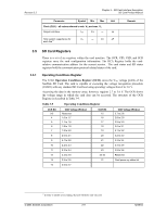
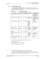
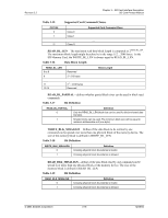
Revision 2.2 Chapter 3 - SD Card Interface Description SD Card Product Manual 3.5.3 Card Specific Data Register The Card Specific Data (CSD) Register configuration information is required to access the card data. In Table 3-11, the Cell Type column defines the CSD field as read-only (R), one-time programmable (R/W) or erasable (R/W/E). The values are presented in "real world" units for each field and coded according to the CSD structure. Table 3-11 CSD Register Fields Field CSD_ STRUCTURE --- TAAC Width 2 6 8 Cell Type R R R CSD Slice [127: 126] [125: 120] [119: 112] CSD Value 1.0 --1.5 msec CSD Code Description 0 CSD structure 000000b Reserved 00100110 Data read access time-1 NSAC 8 R TRANS_ 8 R SPEED CCC 12 R READ_BL_ 4 R LEN READ_BL_ 1 R PARTIAL WRITE_BLK_ 1 R MISALIGN READ_BLK_ 1 R MISALIGN DSR_IMP 1 R --C_SIZE 2 R 12 R VDD_R_ 3 R CURR_MIN VDD_R_ 3 R CURR_MAX [111: 0 104] [103:96] Default 25MHz High-speed 50MHz [95:84] All (inc. WP, lock/unlock) [83:80] 2G Up to 1G [79:79] Yes [78:78] No [77:77] No [76:76] No [75:74] [73:62] [61:59] --- 2 GB 1 GB 512 MB 256 MB 128 MB 64 MB 32 MB 16 MB 100 mA [58:56] 80 mA 00000000b 0110010 01011010 Data read access time-2 in CLK cycles (NSAC*100) Max. data transfer rate 5F5 Ah 9h 1b 0b 0b 0b 00b F24h F22h F1Eh F13h F03h EDFh 74Bh 383h 111b 110b Card command classes Max. read data block length Partial blocks for read allowed Write block misalignment Read block misalignment DSR implemented Reserved Device size Max. read current @VDD min. Max. read current @VDD © 2004 SanDisk Corporation 3-13 12/08/04
-
 1
1 -
2
-
3
-
4
-
5
-
6
-
7
-
8
-
9
-
10
-
11
-
12
-
13
-
14
-
15
-
16
-
17
-
18
-
19
-
20
-
21
-
22
-
23
-
24
-
25
-
26
-
27
-
 28
28 -
 29
29 -
 30
30 -
 31
31 -
 32
32 -
 33
33 -
 34
34 -
 35
35 -
 36
36 -
 37
37 -
 38
38 -
39
-
40
-
41
-
42
-
43
-
44
-
45
-
46
-
47
-
48
-
49
-
50
-
51
-
52
-
53
-
54
-
55
-
56
-
57
-
58
-
59
-
60
-
61
-
62
-
63
-
64
-
65
-
66
-
67
-
68
-
69
-
70
-
71
-
72
-
73
-
74
-
75
-
76
-
77
-
78
-
79
-
80
-
81
-
82
-
83
-
84
-
85
-
86
-
87
-
88
-
89
-
90
-
91
-
92
-
93
-
94
-
95
-
96
-
97
-
98
-
99
-
100
-
101
-
102
-
103
-
104
-
105
-
106
-
107
-
108
-
109
-
110
-
111
-
112
-
113
-
114
-
115
-
116
-
117
-
118
-
119
-
120
-
121
-
122
-
123
 |
 |
