SanDisk SDSDH-1024 Product Manual - Page 86
Timing Diagrams
 |
UPC - 710348911073
View all SanDisk SDSDH-1024 manuals
Add to My Manuals
Save this manual to your list of manuals |
Page 86 highlights
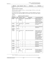
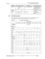
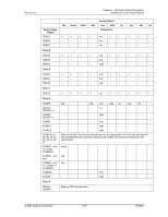
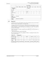
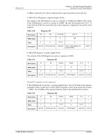
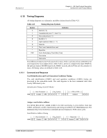
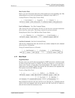
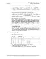
Revision 2.2 Chapter 4 - SD Card Protocol Description SanDisk SD Card Product Manual 4.10 Timing Diagrams All timing diagrams use schematics and abbreviations listed in Table 4-23. Table 4-23 Timing Diagram Symbols Symbol Definition S Start Bit (= 0) T Transmitter Bit (Host = 1, Card = 0) P One-cycle pull-up (= 1) E End Bit (= 1) Z High Impedance State (-> = 1) D Data bits X "Don't care" data bits from card * Repetition CRC Cyclic Redundancy Check Bits (7 bits) Card active Host active The difference between the P-bit and Z-bit is that a P-bit is actively driven to HIGH by the card respectively host output driver, while Z-bit is driven to (respectively kept) HIGH by the pull-up resistors RCMD respectively RDAT. Actively-driven P-bits are less sensitive to noise. All timing values are defined in Table 4-24. 4.10.1 Command and Response Card Identification and Card Operation Conditions Timing The card identification (CMD2) and card operation conditions (CMD1) timing are processed in the open-drain mode. The card response to the host command starts after exactly NID clock cycles. Identification Timing (Card ID Mode) Host Command NIDCycles CMD S T Content CRC E Z Z P *** PST CID or OCR Content ZZZ Assign a card relative address The SEND_RELATIVE_ADDR (CMD 3) for SD Card timing is given bellow. Note that CMD3 command's content, functionality and timing are different for MultiMediaCard. The minimum delay between the host command and card response is NCR clock cycles. Send Relative Address Timing Host Command NCRCycles CMD S T Content CRC E Z Z P *** Response P S T Content CRC Z E Z Z Z © 2004 SanDisk Corporation 4-42 12/08/04
-
 1
1 -
2
-
3
-
4
-
5
-
6
-
7
-
8
-
9
-
10
-
11
-
12
-
13
-
14
-
15
-
16
-
17
-
18
-
19
-
20
-
21
-
22
-
23
-
24
-
25
-
26
-
27
-
28
-
29
-
30
-
31
-
32
-
33
-
34
-
35
-
36
-
37
-
38
-
39
-
40
-
41
-
42
-
43
-
44
-
45
-
46
-
47
-
48
-
49
-
50
-
51
-
52
-
53
-
54
-
55
-
56
-
57
-
58
-
59
-
60
-
61
-
62
-
63
-
64
-
65
-
66
-
67
-
68
-
69
-
70
-
71
-
72
-
73
-
74
-
75
-
76
-
77
-
78
-
79
-
80
-
 81
81 -
 82
82 -
 83
83 -
 84
84 -
 85
85 -
 86
86 -
 87
87 -
 88
88 -
 89
89 -
 90
90 -
 91
91 -
92
-
93
-
94
-
95
-
96
-
97
-
98
-
99
-
100
-
101
-
102
-
103
-
104
-
105
-
106
-
107
-
108
-
109
-
110
-
111
-
112
-
113
-
114
-
115
-
116
-
117
-
118
-
119
-
120
-
121
-
122
-
123
 |
 |
