Brother International HL-720 Service Manual - Page 106
A 10Kbit FIFO is includedrporated., TIMER 3 Watch Dog
 |
View all Brother International HL-720 manuals
Add to My Manuals
Save this manual to your list of manuals |
Page 106 highlights
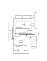
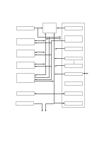
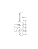
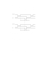
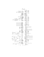
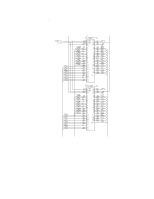
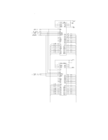
1.3.2 ASIC The ASIC is composed of a Cell Based IC and has the following function blocks. (1) Oscillator circuit Generates the main clock for the CPU by dividing the source clock frequency by two. (2) Address Generator This controls the address buss by latching the AD buss signals with the ALE signal. (3) Address decoder Generates the CS for each device. (4) DRAM control Generates the RAS, CAS, WE, OE and MA signals for the DRAM and controls the memory refresh processing (CAS before RAS self-refreshing method). (5) Interrupt control Interrupt levels: Priority High 9 8 7 6 5 4 3 2 Low 1 TIMER 3 (Watch Dog) MONITOR FIFO EXINT TIMER1 BD Spare CDCC / BOISE / DATA EXTENTION TIMER 2 All the interrupts can be masked. (6) Timers The following timers are included: Timer 1 16-bit timer Timer 2 10-bit timer Timer 3 Watch-dog timer (7) FIFO A 10Kbit FIFO is includedrporated. Data for one raster is transferred from the RAM to the FIFO by DMA transmission and is output as serial video data. The data cycle is 6.13 Mhz. II-4
-
 1
1 -
2
-
3
-
4
-
5
-
6
-
7
-
8
-
9
-
10
-
11
-
12
-
13
-
14
-
15
-
16
-
17
-
18
-
19
-
20
-
21
-
22
-
23
-
24
-
25
-
26
-
27
-
28
-
29
-
30
-
31
-
32
-
33
-
34
-
35
-
36
-
37
-
38
-
39
-
40
-
41
-
42
-
43
-
44
-
45
-
46
-
47
-
48
-
49
-
50
-
51
-
52
-
53
-
54
-
55
-
56
-
57
-
58
-
59
-
60
-
61
-
62
-
63
-
64
-
65
-
66
-
67
-
68
-
69
-
70
-
71
-
72
-
73
-
74
-
75
-
76
-
77
-
78
-
79
-
80
-
81
-
82
-
83
-
84
-
85
-
86
-
87
-
88
-
89
-
90
-
91
-
92
-
93
-
94
-
95
-
96
-
97
-
98
-
99
-
100
-
 101
101 -
 102
102 -
 103
103 -
 104
104 -
 105
105 -
 106
106 -
 107
107 -
 108
108 -
 109
109 -
 110
110 -
 111
111 -
112
-
113
-
114
-
115
-
116
-
117
-
118
-
119
-
120
-
121
-
122
-
123
-
124
-
125
-
126
-
127
-
128
-
129
-
130
-
131
-
132
-
133
-
134
-
135
-
136
-
137
-
138
-
139
-
140
-
141
-
142
-
143
-
144
-
145
-
146
-
147
-
148
-
149
-
150
-
151
-
152
-
153
-
154
 |
 |