Brother International HL-720 Service Manual - Page 27
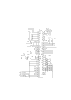
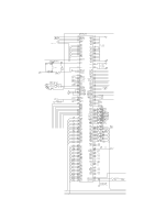
Cdcc / Boise / Data Extention, Exintoption Serial I/o
 |
View all Brother International HL-720 manuals
Add to My Manuals
Save this manual to your list of manuals |
Page 27 highlights
The ASIC is composed of Cell Based IC and has the following function blocks. (1) Oscillator circuit Generates the main clock for the CPU by dividing the source clock frequency into two. (2) Address decoder Generates the CS for each device. (3) DRAM control Generates the RAS, CAS, WE, OE and MA signals for the DRAM and controls refresh recessing (CAS before RAS self-refreshing method). (4) Interrupt control Interrupt levels: Priority High 7 6 5 4 3 2 Low 1 NMI FIFO EXINT(Option Serial I/O) BD / Timer 1 SCANINT CDCC / BOISE / DATA EXTENTION Timer 2 (5) Timers The following timers are incorporated: Timer 1 Timer 2 Timer 3 16-bit timer 10-bit timer Watch-dog timer (6) FIFO A 5,120-bit FIFO is incorporated. Data for one raster is transferred from the RAM to the FIFO by DMA transmission and is output as serial video data. The data cycle is 6.13 MHz. II-10
-
 1
1 -
2
-
3
-
4
-
5
-
6
-
7
-
8
-
9
-
10
-
11
-
12
-
13
-
14
-
15
-
16
-
17
-
18
-
19
-
20
-
21
-
 22
22 -
 23
23 -
 24
24 -
 25
25 -
 26
26 -
 27
27 -
 28
28 -
 29
29 -
 30
30 -
 31
31 -
 32
32 -
33
-
34
-
35
-
36
-
37
-
38
-
39
-
40
-
41
-
42
-
43
-
44
-
45
-
46
-
47
-
48
-
49
-
50
-
51
-
52
-
53
-
54
-
55
-
56
-
57
-
58
-
59
-
60
-
61
-
62
-
63
-
64
-
65
-
66
-
67
-
68
-
69
-
70
-
71
-
72
-
73
-
74
-
75
-
76
-
77
-
78
-
79
-
80
-
81
-
82
-
83
-
84
-
85
-
86
-
87
-
88
-
89
-
90
-
91
-
92
-
93
-
94
-
95
-
96
-
97
-
98
-
99
-
100
-
101
-
102
-
103
-
104
-
105
-
106
-
107
-
108
-
109
-
110
-
111
-
112
-
113
-
114
-
115
-
116
-
117
-
118
-
119
-
120
-
121
-
122
-
123
-
124
-
125
-
126
-
127
-
128
-
129
-
130
-
131
-
132
-
133
-
134
-
135
-
136
-
137
-
138
-
139
-
140
-
141
-
142
-
143
-
144
-
145
-
146
-
147
-
148
-
149
-
150
-
151
-
152
-
153
-
154
 |
 |