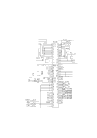
Brother International HL-720 Service Manual - Page 20
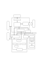
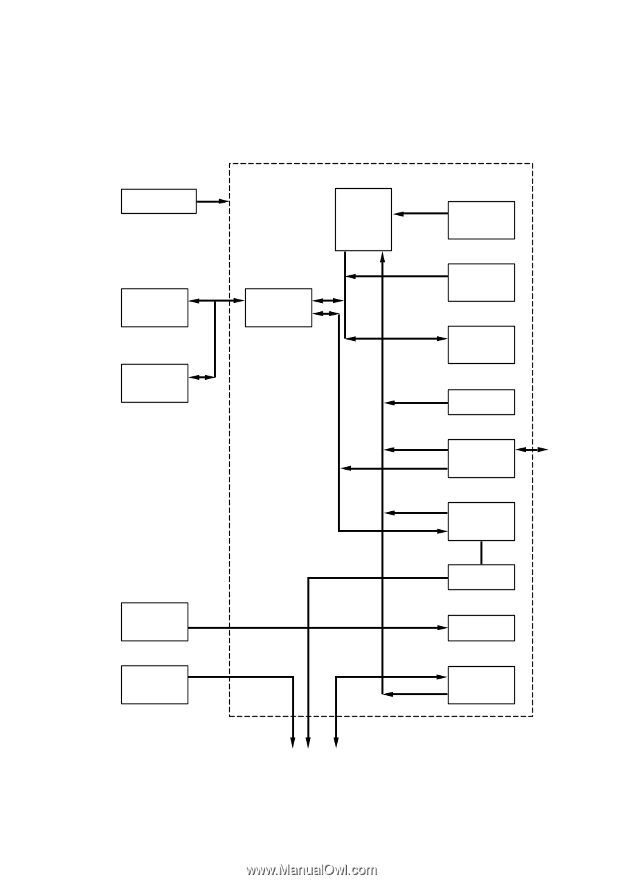
Main PCB Block Diagram, <HL-720>, Fig. 2.3, Fig. 2.3 shows a block diagram of the main PCB.
 |
View all Brother International HL-720 manuals
Add to My Manuals
Save this manual to your list of manuals |
Page 20 highlights
1.2 Main PCB Block Diagram Fig. 2.3 shows a block diagram of the main PCB. ASIC Reset Circuit CPU Core (Z80) BUS INT DRAM 0.5 Mbytes Option RAM 1.5 Mbytes or 3.5 Mbytes DRAM Control EEPROM (128 x 8 bits) Motor Driver To Panel sensor PCB Fig. 2.3 II-3 Oscillator (12.27 MHz) Program ROM 16 Kbytes Working S-RAM 512 Bytes Timer CDCC Parallel I/O To PC DATA Extension FIFO EEPROM I/O Engine Control I/O
-
 1
1 -
2
-
3
-
4
-
5
-
6
-
7
-
8
-
9
-
10
-
11
-
12
-
13
-
14
-
 15
15 -
 16
16 -
 17
17 -
 18
18 -
 19
19 -
 20
20 -
 21
21 -
 22
22 -
 23
23 -
 24
24 -
 25
25 -
26
-
27
-
28
-
29
-
30
-
31
-
32
-
33
-
34
-
35
-
36
-
37
-
38
-
39
-
40
-
41
-
42
-
43
-
44
-
45
-
46
-
47
-
48
-
49
-
50
-
51
-
52
-
53
-
54
-
55
-
56
-
57
-
58
-
59
-
60
-
61
-
62
-
63
-
64
-
65
-
66
-
67
-
68
-
69
-
70
-
71
-
72
-
73
-
74
-
75
-
76
-
77
-
78
-
79
-
80
-
81
-
82
-
83
-
84
-
85
-
86
-
87
-
88
-
89
-
90
-
91
-
92
-
93
-
94
-
95
-
96
-
97
-
98
-
99
-
100
-
101
-
102
-
103
-
104
-
105
-
106
-
107
-
108
-
109
-
110
-
111
-
112
-
113
-
114
-
115
-
116
-
117
-
118
-
119
-
120
-
121
-
122
-
123
-
124
-
125
-
126
-
127
-
128
-
129
-
130
-
131
-
132
-
133
-
134
-
135
-
136
-
137
-
138
-
139
-
140
-
141
-
142
-
143
-
144
-
145
-
146
-
147
-
148
-
149
-
150
-
151
-
152
-
153
-
154
 |
 |
II-3
1.2
Main PCB Block Diagram
<HL-720>
Fig. 2.3 shows a block diagram of the main PCB.
Reset Circuit
DRAM
0.5 Mbytes
Option RAM
1.5 Mbytes or
3.5 Mbytes
EEPROM
(128 x 8 bits)
DRAM Control
Oscillator
(12.27 MHz)
Program ROM
16 Kbytes
Working S-RAM
512 Bytes
Timer
CDCC
Parallel
I/O
DATA
Extension
FIFO
EEPROM
I/O
Engine
Control
I/O
To Panel sensor PCB
To PC
ASIC
CPU Core
(Z80)
BUS
INT
Motor Driver
Fig. 2.3