Oki ML490 Maintenance Manual - Page 133
C-7, C-6
 |
View all Oki ML490 manuals
Add to My Manuals
Save this manual to your list of manuals |
Page 133 highlights
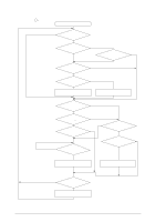
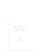
A Yes Are ALE, PSEN, RD, WR, signals as specified in Figure C-6? 180ns 542ns 5V ALE 0V PSEN RD/WR 271ns 5V 0V 542ns 5V 0V Figure C-6 No Replace the Q3. Yes Are (T1) SELECT and (INTO) BUSY signals low level? No Check Q3 on the Control Board. Yes Are +9V and -9V input to Q1? No Replace defective component in +9/-9 volt control circuit. Yes Is pin 1 SSD signal of Q3 High level? No Replace the Q3. Yes Is pin 11 SSD of Q1 low level? No Replace the Q1 or the CN1? Yes Is the RxD of Q3 as specified in Figure C-7? RxD SSD ST bit No Replace the Q2. Yes Replace the Q3. Figure C-7 5V 0V SP bit 5V 0V 42114101 Rev.1 133 /
-
 1
1 -
2
-
3
-
4
-
5
-
6
-
7
-
8
-
9
-
10
-
11
-
12
-
13
-
14
-
15
-
16
-
17
-
18
-
19
-
20
-
21
-
22
-
23
-
24
-
25
-
26
-
27
-
28
-
29
-
30
-
31
-
32
-
33
-
34
-
35
-
36
-
37
-
38
-
39
-
40
-
41
-
42
-
43
-
44
-
45
-
46
-
47
-
48
-
49
-
50
-
51
-
52
-
53
-
54
-
55
-
56
-
57
-
58
-
59
-
60
-
61
-
62
-
63
-
64
-
65
-
66
-
67
-
68
-
69
-
70
-
71
-
72
-
73
-
74
-
75
-
76
-
77
-
78
-
79
-
80
-
81
-
82
-
83
-
84
-
85
-
86
-
87
-
88
-
89
-
90
-
91
-
92
-
93
-
94
-
95
-
96
-
97
-
98
-
99
-
100
-
101
-
102
-
103
-
104
-
105
-
106
-
107
-
108
-
109
-
110
-
111
-
112
-
113
-
114
-
115
-
116
-
117
-
118
-
119
-
120
-
121
-
122
-
123
-
124
-
125
-
126
-
127
-
 128
128 -
 129
129 -
 130
130 -
 131
131 -
 132
132 -
 133
133 -
 134
134 -
 135
135
 |
 |

42114101
Rev.1
133 /
No
Replace the Q2.
Yes
Replace the Q3.
A
Yes
Are ALE, PSEN, RD, WR, signals as specified in Figure C-6?
Figure C-7
542ns
180ns
271ns
542ns
5V
0V
5V
0V
5V
0V
ALE
PSEN
RD/WR
Figure C-6
ST bit
SP bit
5V
0V
5V
0V
RxD
SSD
No
Replace the Q3.
Yes
Are (T1) SELECT and (INTO) BUSY signals low level?
No
Check Q3 on the Control Board.
Yes
Are +9V and -9V input to Q1?
No
Replace defective component in +9/–9 volt control circuit.
Yes
Is pin 1 SSD signal of Q3 High level?
No
Replace the Q3.
Yes
Is pin 11 SSD of Q1 low level?
No
Replace the Q1 or the CN1?
Yes
Is the RxD of Q3 as specified in Figure C-7?