Oki ML490 Maintenance Manual - Page 17
Parallel Interface
 |
View all Oki ML490 manuals
Add to My Manuals
Save this manual to your list of manuals |
Page 17 highlights
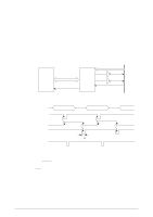
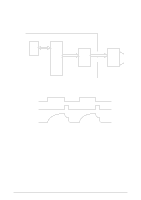
2.1.4 Interface Control (1) Parallel Interface The parallel data input from the host to the interfaced LSI is latched to its internal register at the falling edge of the STROBE-N signal. At the same time, the LSI sets the BUSY signal to the high level to inform the host that the data is being processed, and outputs the RXD signal to inform the MPU of data reception. The data is read upon receiving the RD-N signal from the MPU. When the data processing ends, the BUSY signal is set to off and the ACK-N signal in sent to request the next data. When reception is impossible because the buffer is full, the BUSY signal is sent to request stopping of data transmission. MPU P16 A/D bus RXD-N LSI Receive Data NBSY ACK NSTB NRXD CN1 BUSY ACK-N STROBE-N Receive Data 1 to 8 STROBE-N BUSY ACK-N RXD-N 500ns max. 2~8µs * The STROBE-based timing for the BUSY signal is adjustable from the Maintenance menu. ACK signal timing and BUSY signal timing can be adjusted from the Maintenance menu. 42114101 Rev.1 17 /
-
 1
1 -
2
-
3
-
4
-
5
-
6
-
7
-
8
-
9
-
10
-
11
-
 12
12 -
 13
13 -
 14
14 -
 15
15 -
 16
16 -
 17
17 -
 18
18 -
 19
19 -
 20
20 -
 21
21 -
 22
22 -
23
-
24
-
25
-
26
-
27
-
28
-
29
-
30
-
31
-
32
-
33
-
34
-
35
-
36
-
37
-
38
-
39
-
40
-
41
-
42
-
43
-
44
-
45
-
46
-
47
-
48
-
49
-
50
-
51
-
52
-
53
-
54
-
55
-
56
-
57
-
58
-
59
-
60
-
61
-
62
-
63
-
64
-
65
-
66
-
67
-
68
-
69
-
70
-
71
-
72
-
73
-
74
-
75
-
76
-
77
-
78
-
79
-
80
-
81
-
82
-
83
-
84
-
85
-
86
-
87
-
88
-
89
-
90
-
91
-
92
-
93
-
94
-
95
-
96
-
97
-
98
-
99
-
100
-
101
-
102
-
103
-
104
-
105
-
106
-
107
-
108
-
109
-
110
-
111
-
112
-
113
-
114
-
115
-
116
-
117
-
118
-
119
-
120
-
121
-
122
-
123
-
124
-
125
-
126
-
127
-
128
-
129
-
130
-
131
-
132
-
133
-
134
-
135
 |
 |
