Canon PowerShot 350 Service Manual - Page 37
processing
 |
View all Canon PowerShot 350 manuals
Add to My Manuals
Save this manual to your list of manuals |
Page 37 highlights
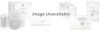
Part 2: Technical Information 1.5 DIGITAL BLOCK D- RAM (4Mbit) FIF0(1Mbit) A/D DRAM Controler FIFO Controler ASIC I SSG Mi-COM I / F OSD Memory Controler DCT 50pin CF Card NTSC Encorder D/A VIDEO SIGNAL EVR RISC- Mi-COM EEPROM CLOCK Battery Levels Fig. 2-5 Digital Block D-RAM: Image data input Image data work memory Still Image Buffer FIFO: Monitor Image Buffer A/D: Converts analog video signal from camera block to a 9 bit digital signal. EVR: Electronic "variable resistor" RISC: Mi-COM: Key Input, System Control and On-screen display (OSD) Image signal processing White balance and exposure compensation control JPEG compression and expansion File management PC Communication (RS232C) Operations controlled through EVR: Flash, Neg/POS signal, self timer, etc. EEPROM: CLOCK: Adjustment Levels Memory Date, Time Battery Levels: Battery level monitor, Auto Power Off ASIC: DCT: Compression and expansion OSD: On-screen Display Information SSG: Video Sync Signal generation 2-5
-
 1
1 -
2
-
3
-
4
-
5
-
6
-
7
-
8
-
9
-
10
-
11
-
12
-
13
-
14
-
15
-
16
-
17
-
18
-
19
-
20
-
21
-
22
-
23
-
24
-
25
-
26
-
27
-
28
-
29
-
30
-
31
-
 32
32 -
 33
33 -
 34
34 -
 35
35 -
 36
36 -
 37
37 -
 38
38 -
 39
39 -
 40
40 -
 41
41 -
 42
42 -
43
-
44
-
45
-
46
-
47
-
48
-
49
-
50
-
51
-
52
-
53
-
54
-
55
-
56
-
57
-
58
-
59
-
60
-
61
-
62
-
63
-
64
-
65
-
66
-
67
-
68
-
69
-
70
-
71
-
72
-
73
-
74
-
75
-
76
-
77
-
78
-
79
-
80
-
81
-
82
-
83
-
84
-
85
-
86
-
87
-
88
-
89
-
90
-
91
-
92
-
93
-
94
-
95
-
96
-
97
-
98
-
99
-
100
-
101
-
102
-
103
-
104
-
105
-
106
-
107
-
108
-
109
-
110
-
111
-
112
-
113
-
114
-
115
-
116
-
117
-
118
-
119
-
120
-
121
-
122
-
123
-
124
-
125
-
126
-
127
-
128
-
129
-
130
-
131
-
132
-
133
-
134
-
135
-
136
-
137
-
138
-
139
 |
 |