Canon PowerShot 350 Service Manual - Page 39
Internal, Associated, Circuits
 |
View all Canon PowerShot 350 manuals
Add to My Manuals
Save this manual to your list of manuals |
Page 39 highlights
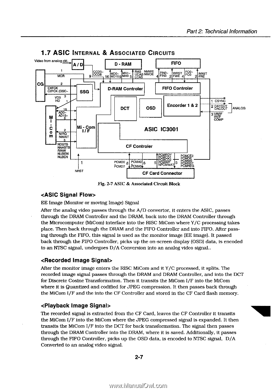
Part 2: Technical Information 1.7 ASIC INTERNAL & ASSOCIATED CIRCUITS I Video from analog ckt. A1D 1 MCR CG 2 EXFCK C2FCK (OSC- VD3 HD SSG ADO-6 AD15- 6 D - RAM FIFO A CCDOCCD8 16 mpo_ aMA1MD159 MAn' A RAS NMWE CAS NWOE LUCAS 4 FINOFINS 2 WRST FWE 4 OF3 RRST 2 FRE • • D-RAM Controler FIFO Controler DCT OSD Encorder 1 & 2 1 CSYNC 2 DAYOUT DACOUT 3 VREF IREF COMP ANALOG C 0 m 2 NIRQ NWAIT 5 NDSTB NAASTB FUNW NUBEN NLBEN Mi - CFom I / NRST ASIC IC3001 CF Controler PCMDO PCMD7 PCMAO 6 i5cmA6-, pPCprMoRpDoYi PL,11/K,D2 PcMcE2 Pp umMwuEE 5 PN$MCMWWPAT 5 P MRST P MREG CF Card Connector Fig. 2-7 ASIC & Associated Circuit Block EE Image (Monitor or moving Image) Signal After the analog video passes through the A/D convertor, it enters the ASIC, passes through the DRAM Controller and the DRAM, back into the DRAM Controller through the Microcomputer (MiCom) interface into the RISC MiCom where Y/C processing takes place. Then back through the DRAM and the FIFO Controller and into FIFO. After passing through the FIFO, this signal is used as the monitor image (EE image). It passed back through the FIFO Controller, picks up the on-screen display (OSD) data, is encoded to an NTSC signal, undergoes D/A Conversion into an analog video signal.. After the monitor image enters the RISC MiCom and it Y/C processed, it splits. The recorded image signal passes through the DRAM and DRAM Controller, and into the DCT for Discrete Cosine Transformation. Then it transits the MiCom I/F into the MiCom where it is Quantized and codified for JPEG compression. It then passes back through the MiCom I/F and the into the CF Controller and stored in the CF Card flash memory. The recorded signal is extracted from the CF Card, leaves the CF Controller it transits the MiCom I/F into the MiCom where the JPEG compressed signal is expanded. It then transits the MiCom I/F into the DCT for back transformation. The signal then passes through the DRAM Controller into the DRAM, where it is saved. Additionally, it passes through the FIFO Controller, picks up the OSD data, is encoded to NTSC signal, D/A Converted to an analog video signal. 2-7
-
 1
1 -
2
-
3
-
4
-
5
-
6
-
7
-
8
-
9
-
10
-
11
-
12
-
13
-
14
-
15
-
16
-
17
-
18
-
19
-
20
-
21
-
22
-
23
-
24
-
25
-
26
-
27
-
28
-
29
-
30
-
31
-
32
-
33
-
 34
34 -
 35
35 -
 36
36 -
 37
37 -
 38
38 -
 39
39 -
 40
40 -
 41
41 -
 42
42 -
 43
43 -
 44
44 -
45
-
46
-
47
-
48
-
49
-
50
-
51
-
52
-
53
-
54
-
55
-
56
-
57
-
58
-
59
-
60
-
61
-
62
-
63
-
64
-
65
-
66
-
67
-
68
-
69
-
70
-
71
-
72
-
73
-
74
-
75
-
76
-
77
-
78
-
79
-
80
-
81
-
82
-
83
-
84
-
85
-
86
-
87
-
88
-
89
-
90
-
91
-
92
-
93
-
94
-
95
-
96
-
97
-
98
-
99
-
100
-
101
-
102
-
103
-
104
-
105
-
106
-
107
-
108
-
109
-
110
-
111
-
112
-
113
-
114
-
115
-
116
-
117
-
118
-
119
-
120
-
121
-
122
-
123
-
124
-
125
-
126
-
127
-
128
-
129
-
130
-
131
-
132
-
133
-
134
-
135
-
136
-
137
-
138
-
139
 |
 |