Epson 2070 Service Manual - Page 70
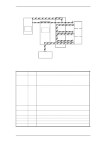
CONTROL CIRCUIT, Overview of Control Circuit Operation, Control Circuit Block Diagram
 |
UPC - 010343812277
View all Epson 2070 manuals
Add to My Manuals
Save this manual to your list of manuals |
Page 70 highlights
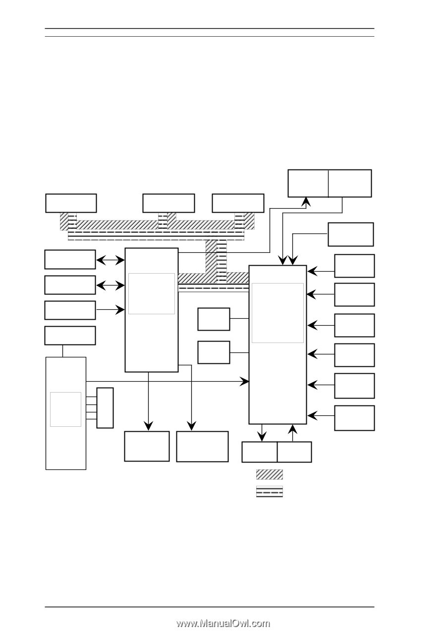
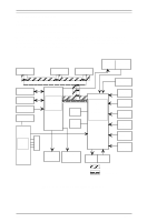
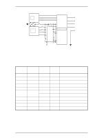
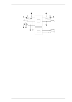
Operation Principles LQ-2070 Servcie Manual 2.3 CONTROL CIRCUIT The control circuit consists of the C186 MAIN board assembly and C165 PNL board This section describes the major components and explains how the boards work. 2.3.1 Overview of Control Circuit Operation The printer's control circuit includes a TMP96C041AF CPU that runs at 17.20 MHz, an E05B24YA gate array, a 1M bit PS-RAM (8-bit bus, less than 100ns) , a 2M bit PROM (8-bit bus, less than 100ns), 4M CG (Standard Version) or 8M CG (NLSP Version). It oversees control of all the components in the printer. The following chart shows you a block diagram of the control circuit. Type B I/F IC 3 ROM IC 5 RAM Q1~Q24 Head Temp. Head Drv. Detector Parallel I/F Panel LED Panel SW Power SW PSC PWDN 5V P/ S GL Unit 35V GP IC2 Gate Array E05B24YA IC 8 EEPROM IC 10 Rest IC IC 12 CR Drv. SLA7024M IC 11, IC14 PF Drv. TEA3718SDP +35V Voltage Detector PE-Rear Detector IC 1 CPU TMP96C041AF PE-Front Detector P-Width Detector Home Detector Release Lever Detector Gap Lever Detector CSF Drv. CSF Detector : Data Bus : Address Bus Figure 2-30 Control Circuit Block Diagram 2-22 Rev.A
-
 1
1 -
2
-
3
-
4
-
5
-
6
-
7
-
8
-
9
-
10
-
11
-
12
-
13
-
14
-
15
-
16
-
17
-
18
-
19
-
20
-
21
-
22
-
23
-
24
-
25
-
26
-
27
-
28
-
29
-
30
-
31
-
32
-
33
-
34
-
35
-
36
-
37
-
38
-
39
-
40
-
41
-
42
-
43
-
44
-
45
-
46
-
47
-
48
-
49
-
50
-
51
-
52
-
53
-
54
-
55
-
56
-
57
-
58
-
59
-
60
-
61
-
62
-
63
-
64
-
 65
65 -
 66
66 -
 67
67 -
 68
68 -
 69
69 -
 70
70 -
 71
71 -
 72
72 -
 73
73 -
 74
74 -
 75
75 -
76
-
77
-
78
-
79
-
80
-
81
-
82
-
83
-
84
-
85
-
86
-
87
-
88
-
89
-
90
-
91
-
92
-
93
-
94
-
95
-
96
-
97
-
98
-
99
-
100
-
101
-
102
-
103
-
104
-
105
-
106
-
107
-
108
-
109
-
110
-
111
-
112
-
113
-
114
-
115
-
116
-
117
-
118
-
119
-
120
-
121
-
122
-
123
-
124
-
125
-
126
-
127
-
128
-
129
-
130
-
131
-
132
-
133
-
134
-
135
-
136
-
137
-
138
-
139
-
140
-
141
-
142
-
143
-
144
-
145
-
146
-
147
-
148
-
149
-
150
-
151
-
152
-
153
-
154
-
155
-
156
-
157
-
158
-
159
-
160
-
161
-
162
-
163
-
164
-
165
 |
 |